Debugging the RAMP GENERATOR
Category: Unknown · Tags: — · Posts: 35
#1 — jestern · 2020-08-09
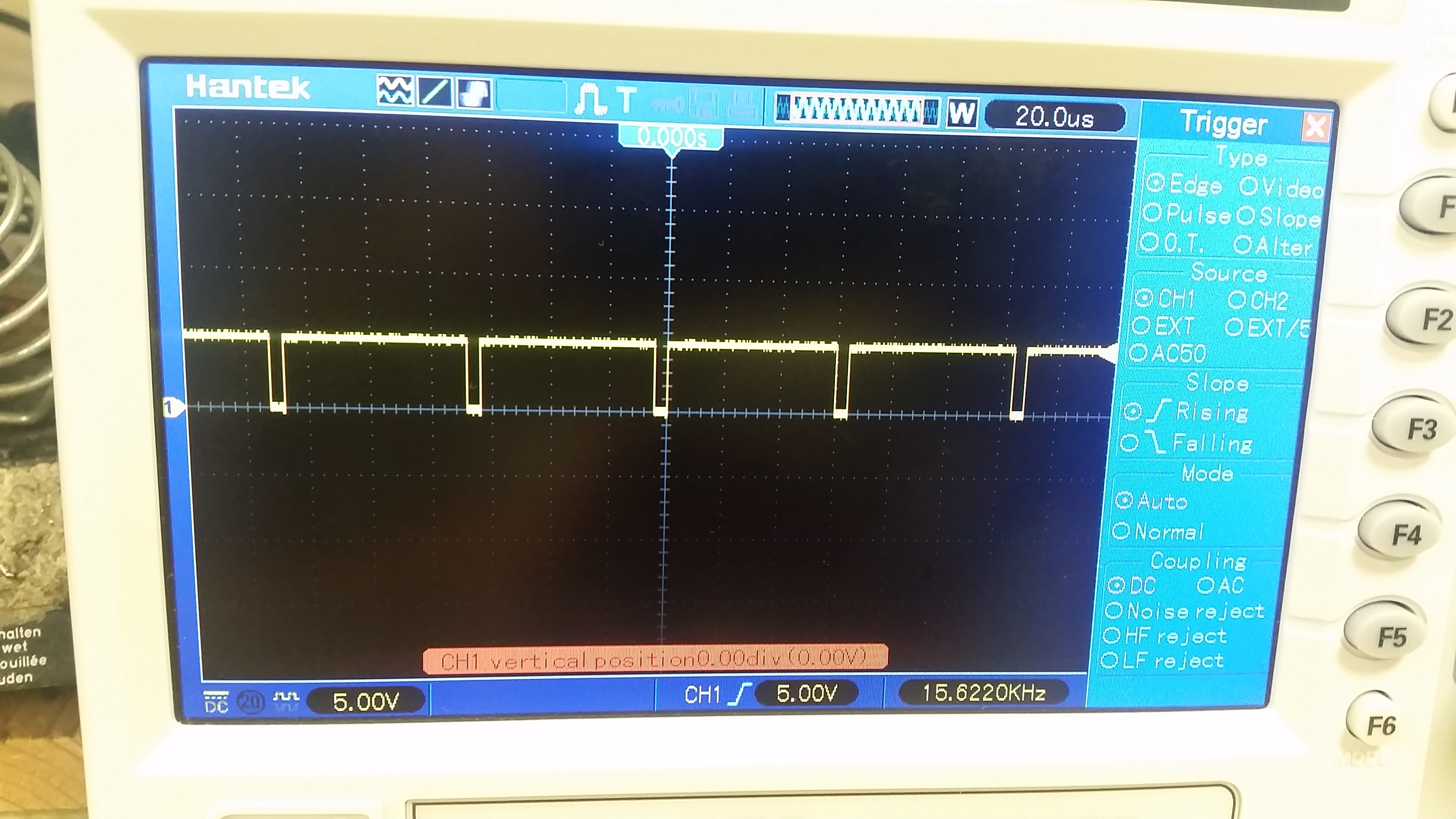
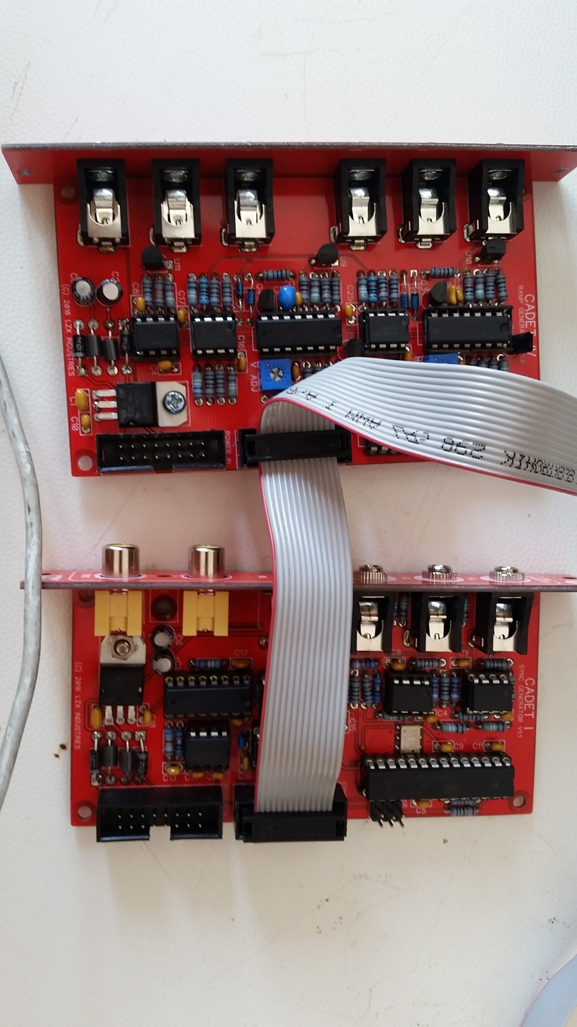
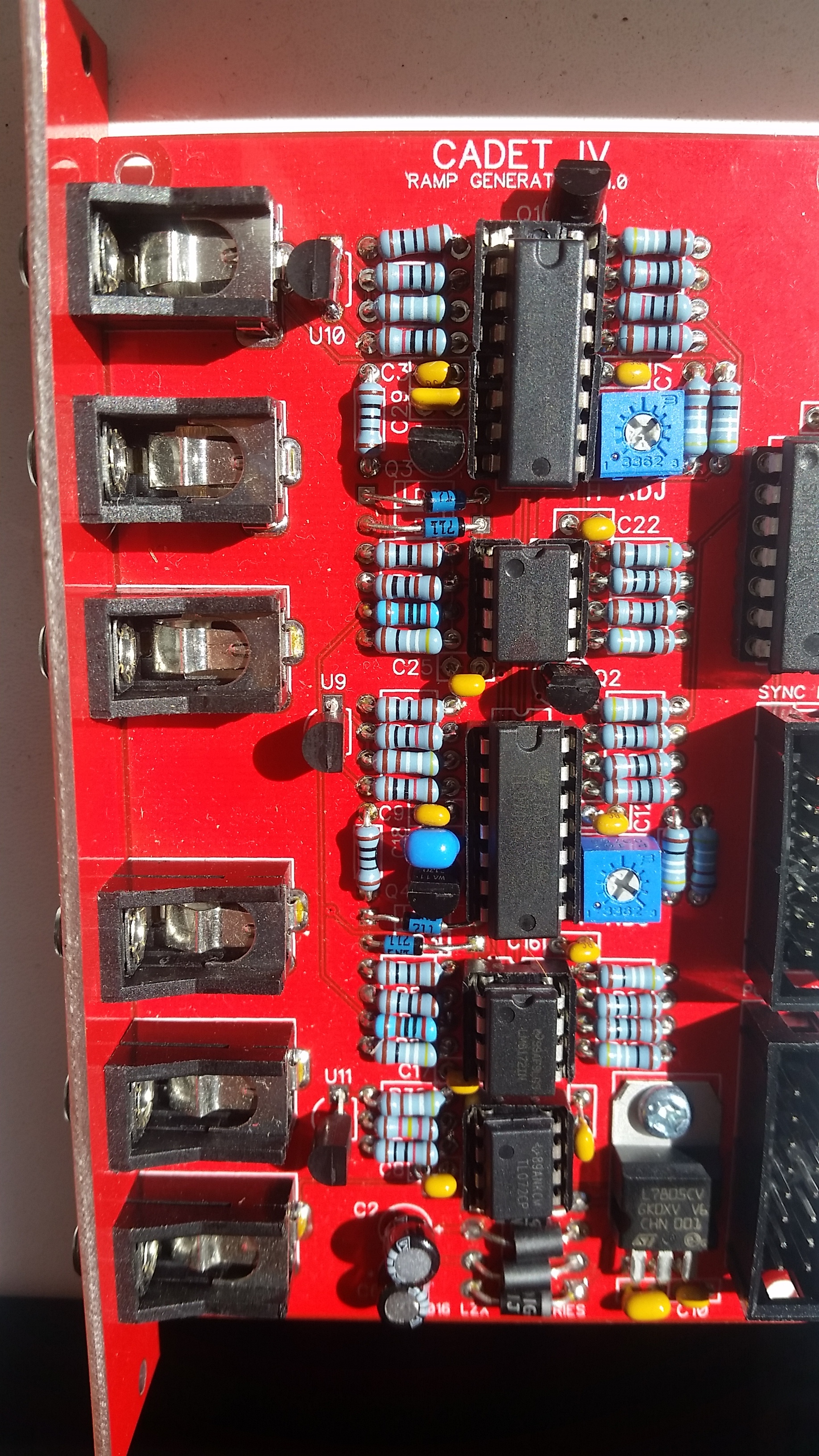
Hi guys my Ramp is not working after the build. I started by checking the Cadet I Sync (I attach some pictures underneath of its signals from the jack outputs and pins of the sync plugs). Does it look normal? Seems ok to me but I don’t know how the sync signals should be. My ramp has flat output on all jacks. Tried changing the ICs and turning the trimpots. All ICs get power (-11 +11 is it maybe too low?). Any idea what could be. Attach all pictures.
JACK OUTPUTS 3 pictures SYNC HEADER PINS 7 pictures + boards and connections
#2 — VisibleSignals · 2020-08-09
Hi Jestern. +/-11V is fine (the IN4001 diodes steal a bit of the 12V from your supply, but that’s fine and normal).
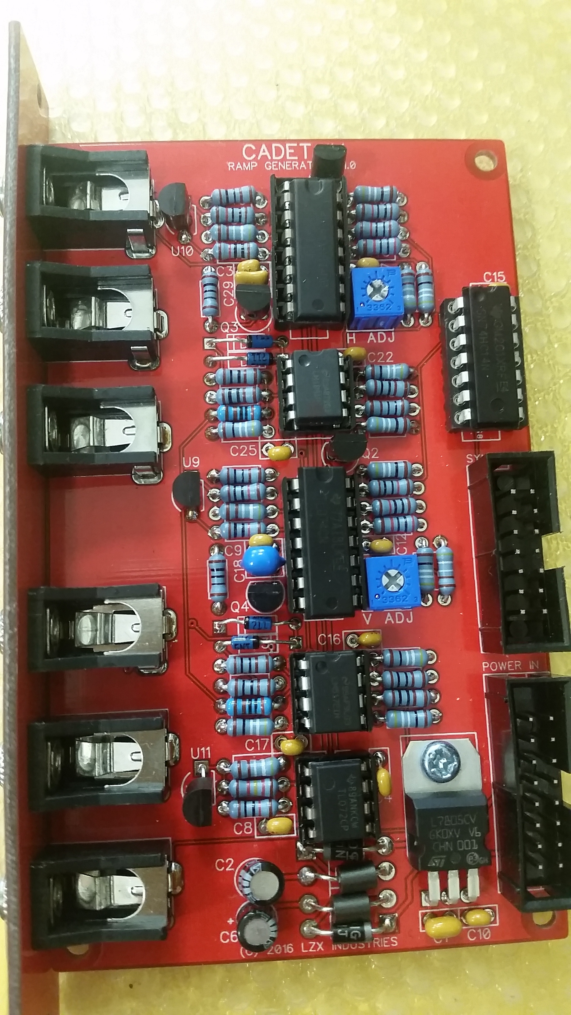
Check out the schematic https://github.com/lzxindustries/documentation/blob/master/Cadet%20IV%20Dual%20Ramp%20Generator/Cadet%20IV%20Dual%20Ramp%20Generator%20Schematics.pdf for information you’ll need to work out what’s wrong. Don’t worry if you don’t understand the details of how the circuit works, just try to get an understanding of how the schematic relates to your PCB and the components you soldered to it.
First check the voltage on all the power pins on all the ICs. You can google the chips to find their datasheets or pinouts to work out which pins are which (“lm6172 datasheet” or “lm6172 pinout”). “V+” or “Vcc” means +11V, “V-” or “Vee” means -11V, ground means 0V. You should check these with the module plugged in to power, but be careful not to accidently short your test lead across two pins - while it’s usually OK sometimes doing that can damage things.
You can also check that ground pins are all connected, by using a multimeter on resistance with the module disconnected from the euro power. Check that the ground pins on the euro power connector (there are lots of them) have nearly no resistance to anywhere you see a ground signal on an IC pin in the schematic.
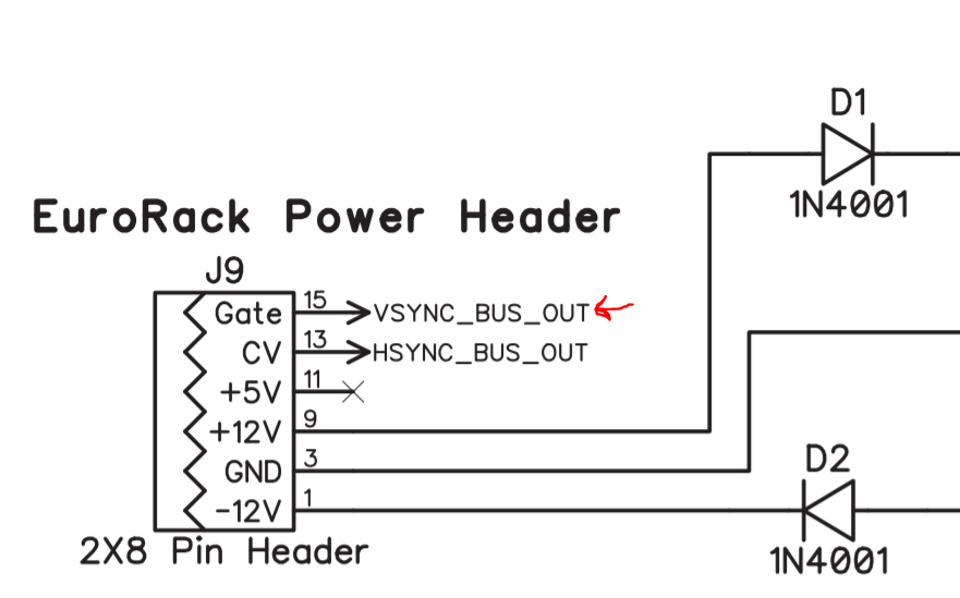
Next, make sure the sync signals are making it to R45 and R27 (i.e. they look the same as they do coming out of the sync module).
Then, see if there’s any ramp on the + input to U13.2 and U12.2.
There’s another thread on the forum recently where someone was having trouble with one of their two ramp outputs - you might find some other helpful debugging advice there.
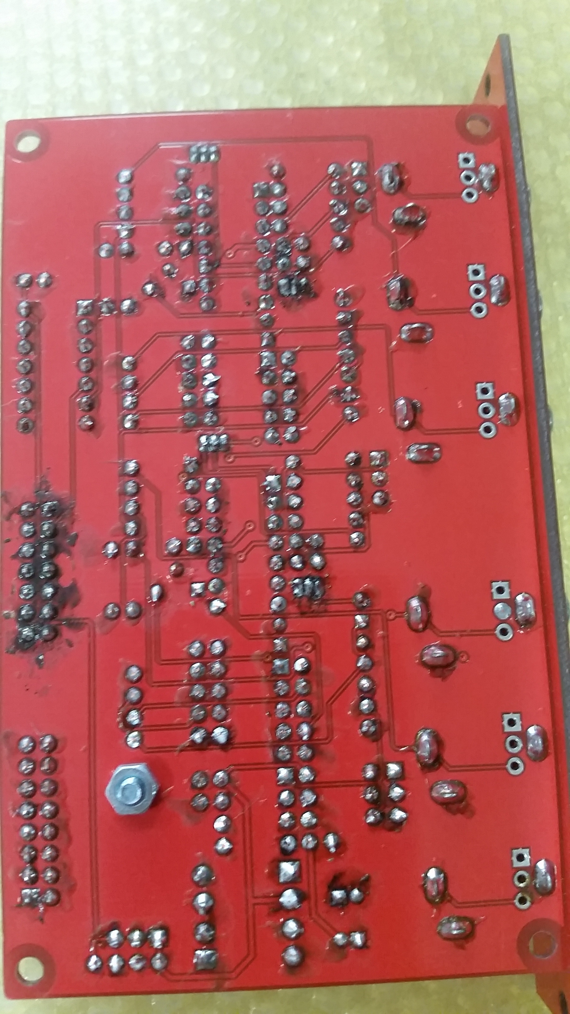
When I zoom in your photos of the PCBs are a bit blurry so it’s a bit hard to comment usefully on them, sorry.
Let us know how you go, there are plenty more things to check!
#3 — jestern · 2020-09-01
Hi Aladan thanks so much for your time in helping me. I finally found the time to check all previous points. this is what I found:
All ICs get the aforementioned power, All ground pins are connected as far as I can see from the schematics.
The TL072 gets +10 and -12 is that ok?
The 74HC14 gets +4.2 and -0.8 on the ground.
Measuring around I noticed a little disparity in the pins of the two LM6172 (few KOhm difference), something around 11k on all right pins of the H lm6172 and 17 Kohm for the ones of the V lm6172. Maybe due to the trimmer?
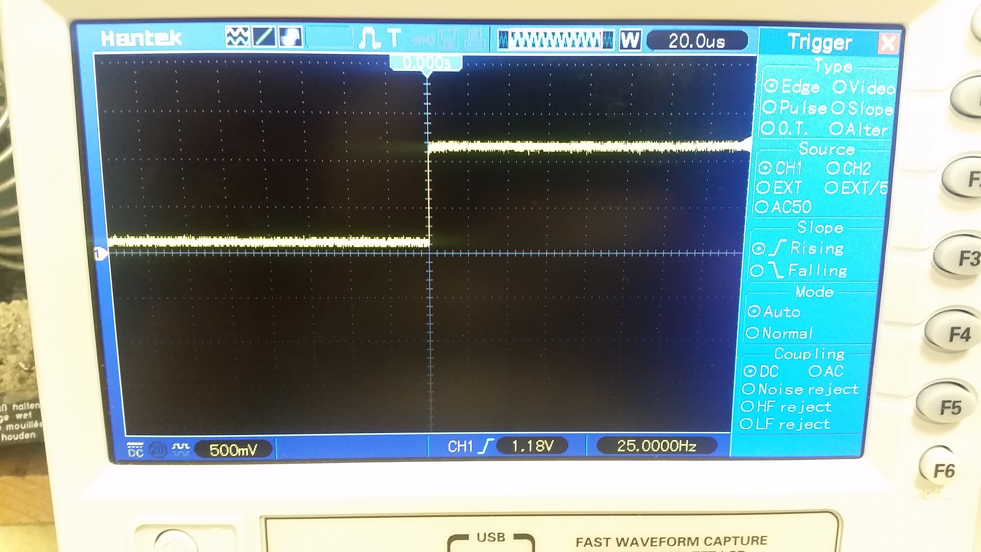
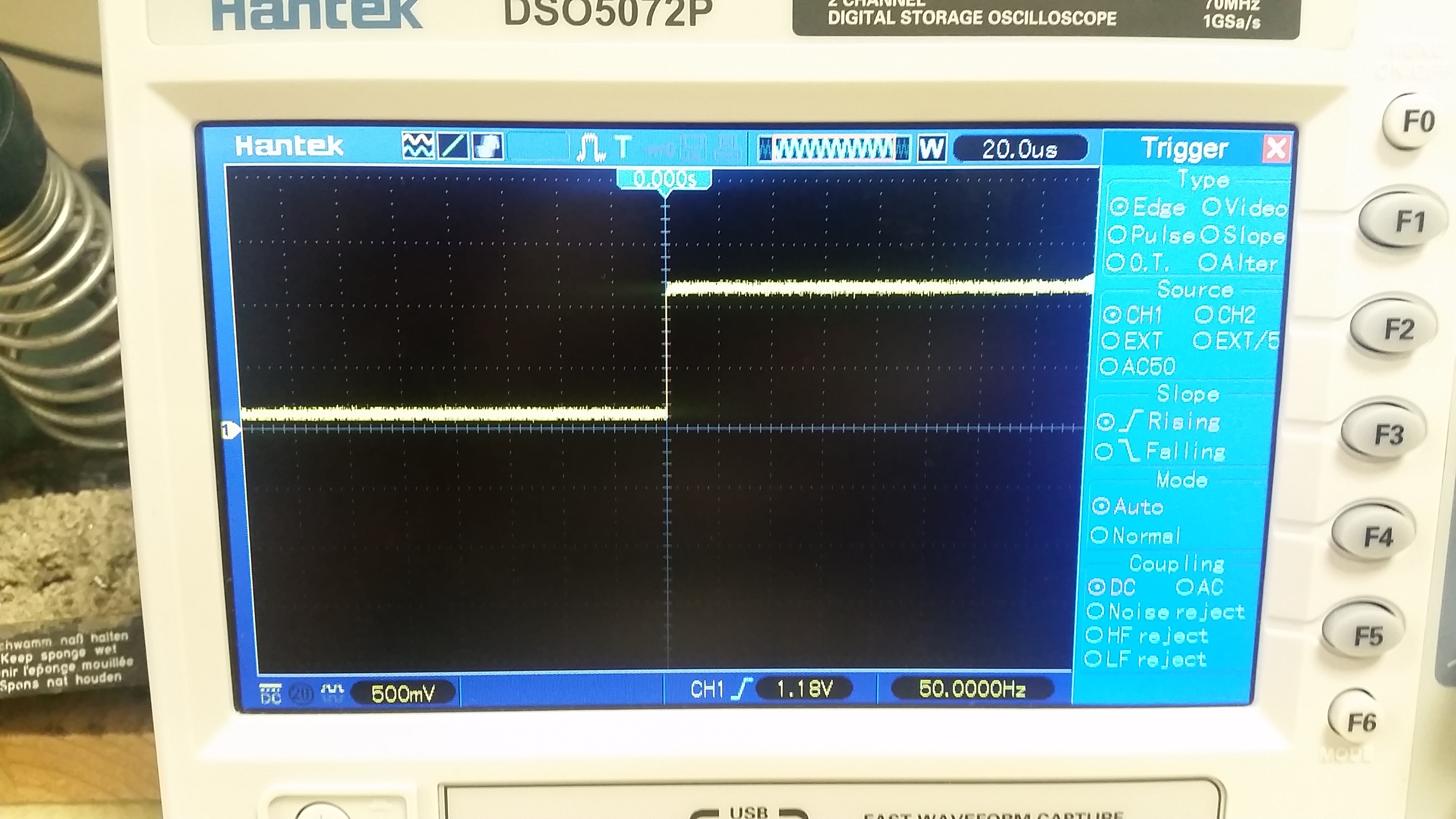
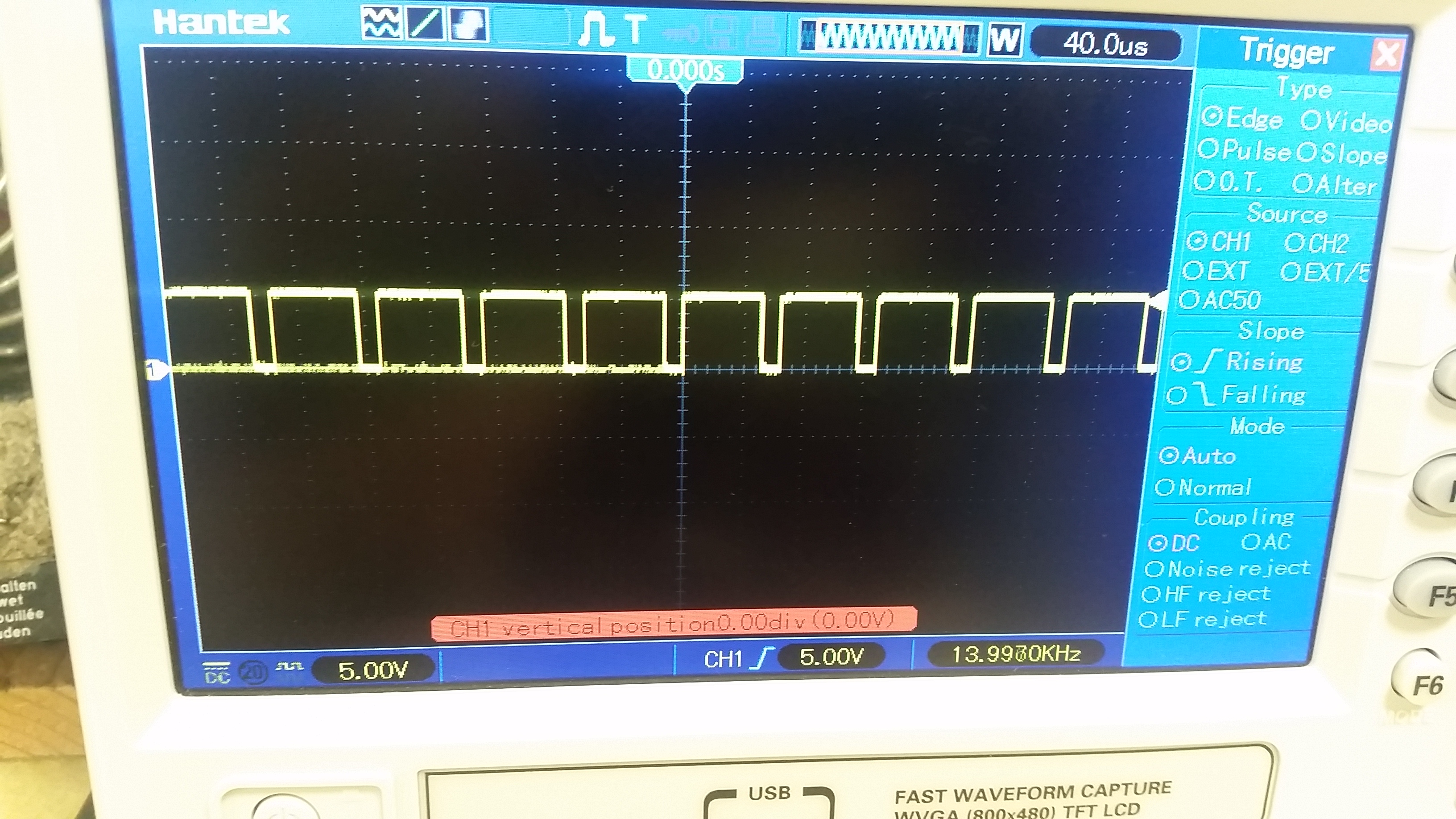
Anyway the sync comes to both resistors 27 and 45. I attach some pictures. on the 45, I think is H sync, is faster than the one on 27.
After that I noticed no signal input at the TL074, I’m not a schematic guru, but I thought U13.2 means the non inverting input of opamp number 2 of the TL074, eg. pin 5, same for U12.2.
So where could the signal get lost?
I attach some pictures of the sync and the boards with better resolution I hope.
Thanks a lot, this keeps me going.
Cheers
Alberto
#4 — Fox · 2020-09-01
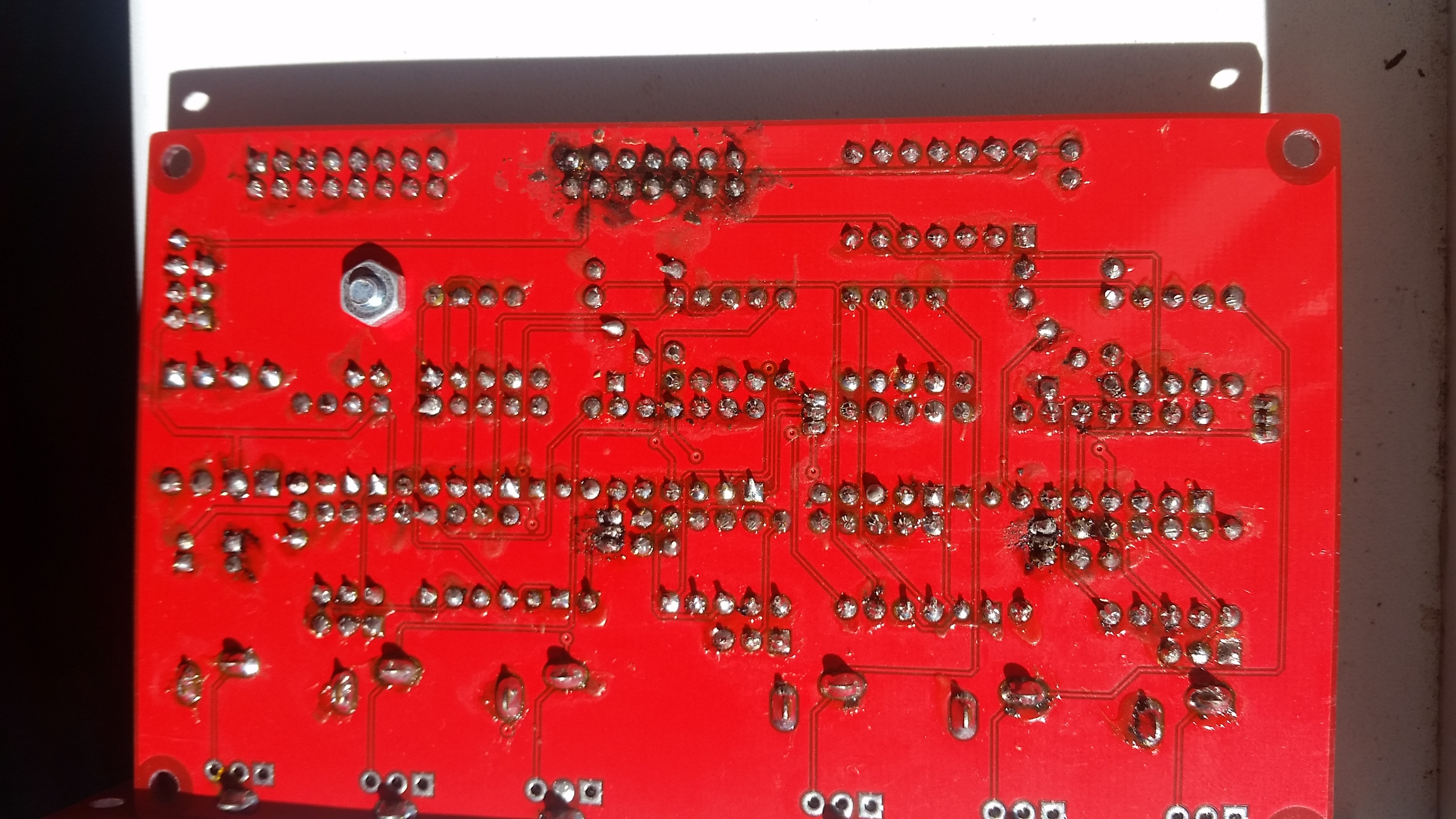
I am not trying to be rude, but can you clean the burned flux between the transistor pins on the bottom of your board? Q1, Q2, Q3 and Q4. I find these footprints are harder to solder than soic chips.
Also double check the text on each transistor to make sure none of the 3906, BS170 or TL431 got switched by mistake. I keep my 3904’s and 3906’s in a drawer next to eachother, so I am always weary of them getting mixed up.
Are you using any substituted parts? A common alternative for the BS170 has a reversed pinout for example.
#5 — Agawell · 2020-09-01
Fox wrote:
I am not trying to be rude, but can you clean the burned flux between the transistor pins on the bottom of your board? Q1, Q2, Q3 and Q4. I find these footprints are harder to solder than soic chips.
completely agree on this definitely looks to be the most suspect area of soldering, but hard to tell!!!
soldering those transistors is horrible - very thin solder and plenty of flux is the answer I suspect
#6 — VisibleSignals · 2020-09-01
Hi Alberto,
Thanks for all that. It’s a little bit surprising that you say the ground pin on the 74HC14 reads -0.8V. It should definitely read 0V, maybe 0.1V at most. Where did you put the other lead of the multimeter when you found that? But I think that just might be an issue with measuring, not with the circuit.
Based on the missing signal at U13.2 pin 5, I agree with what Fox and Agawell said which is that the transistor (Q4, BS170) might be backwards, have a short (solder across two pins) or be an incorrect part, so check that out first.
Other possibilities might be a wrong/faulty capacitor C18, or an issue with the current source (Q2/U13.1/U9). Measuring that might be a little bit tricky, but first could you see what your multimeter says is the voltage between ground (on the power header) and U13.1 pin 3?
Looking at the photo, the TL072 (U1) looks like it could be better seated (pushed down into the socket). But that’s unlikely to be causing the problem you’re seeing.
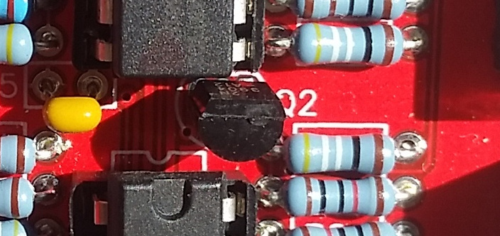
Aha! I think I just found the problem. Q2 is a 2N3904, it should be a 2N3906! You might have swapped it with another transistor…
#7 — VisibleSignals · 2020-09-01
#8 — Fox · 2020-09-02
BINGO!
I cannot believe you spotted that.
#9 — VisibleSignals · 2020-09-02
I am nothing if not meticulous and detail-oriented!

#10 — VisibleSignals · 2020-09-02
Also Alberto, please accept my compliments on your Strange Attractor Sequence - it’s my favourite video of yours (although I just found you now have heaps more on your vimeo that I haven’t look through yet!)
#11 — jestern · 2020-09-02
Alan and everyone thanks so much for spotting this!!! I’ll work on it now and hopefully it’s the only mistake. Thanks so much for the compliments. I started working with lasers but now I’m slowly transitioning towards more video work.
I find more and more this is a great community of incredibly competent and kind people. I hope to contribute back when I have all up and running. I’ll report back when all works fine.
#12 — jestern · 2020-09-02
Thanks I did swap those transistors!!!

My BS170 has a WA 11 written on it before the BS170. How do I know which version is it?
#13 — VisibleSignals · 2020-09-02
Every BS170 should have the same pinout, even if it has other markings. They are batch numbers, year of manufacture codes etc.
#14 — jestern · 2020-09-02
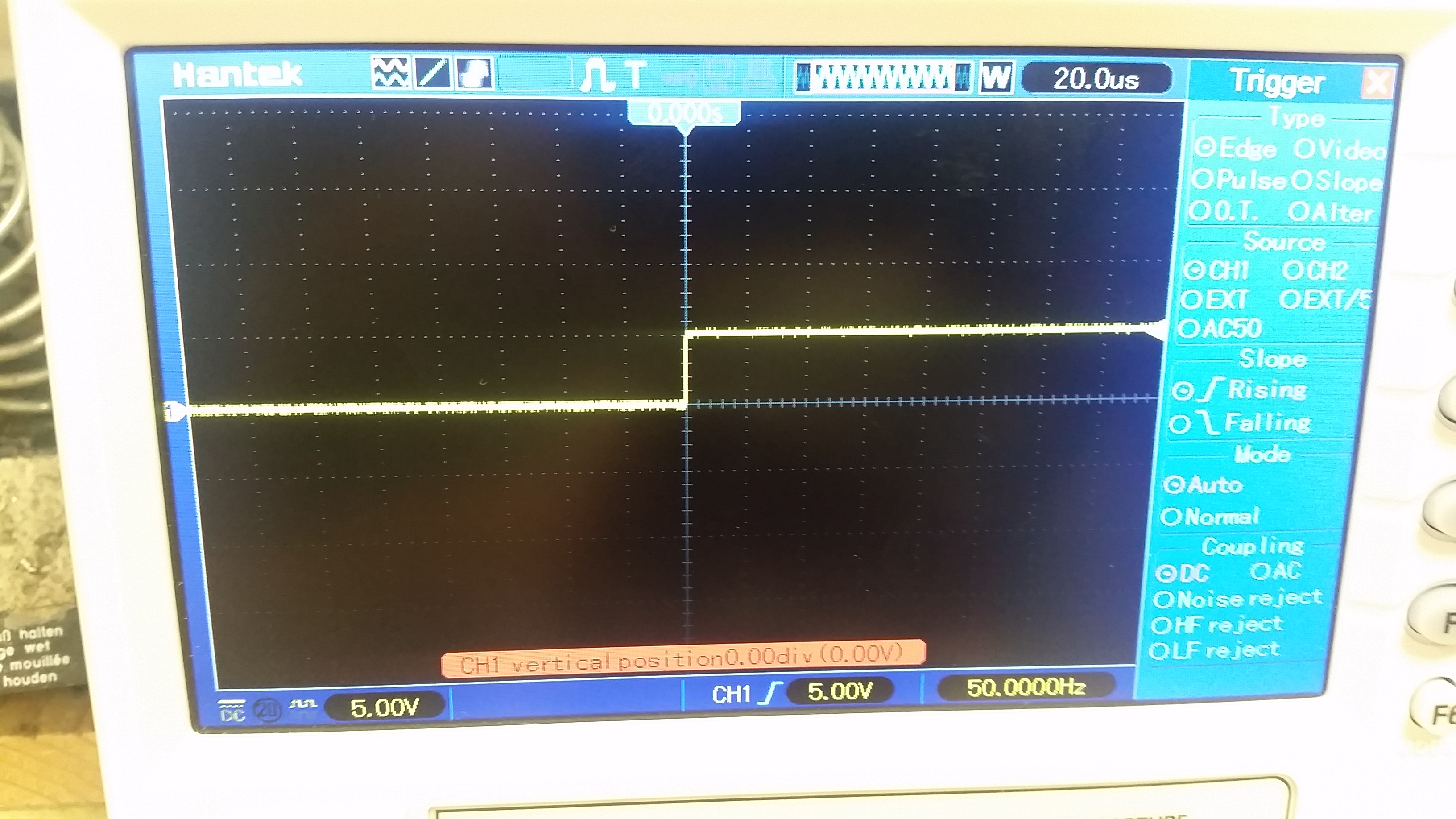
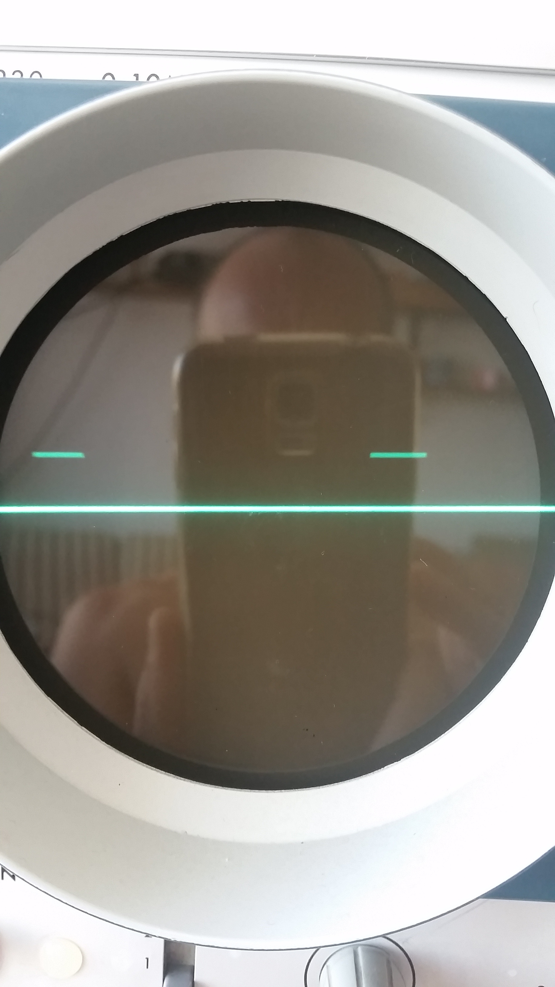
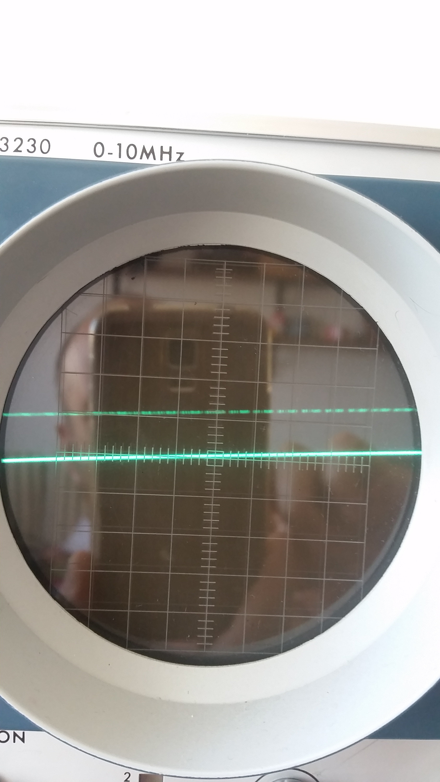
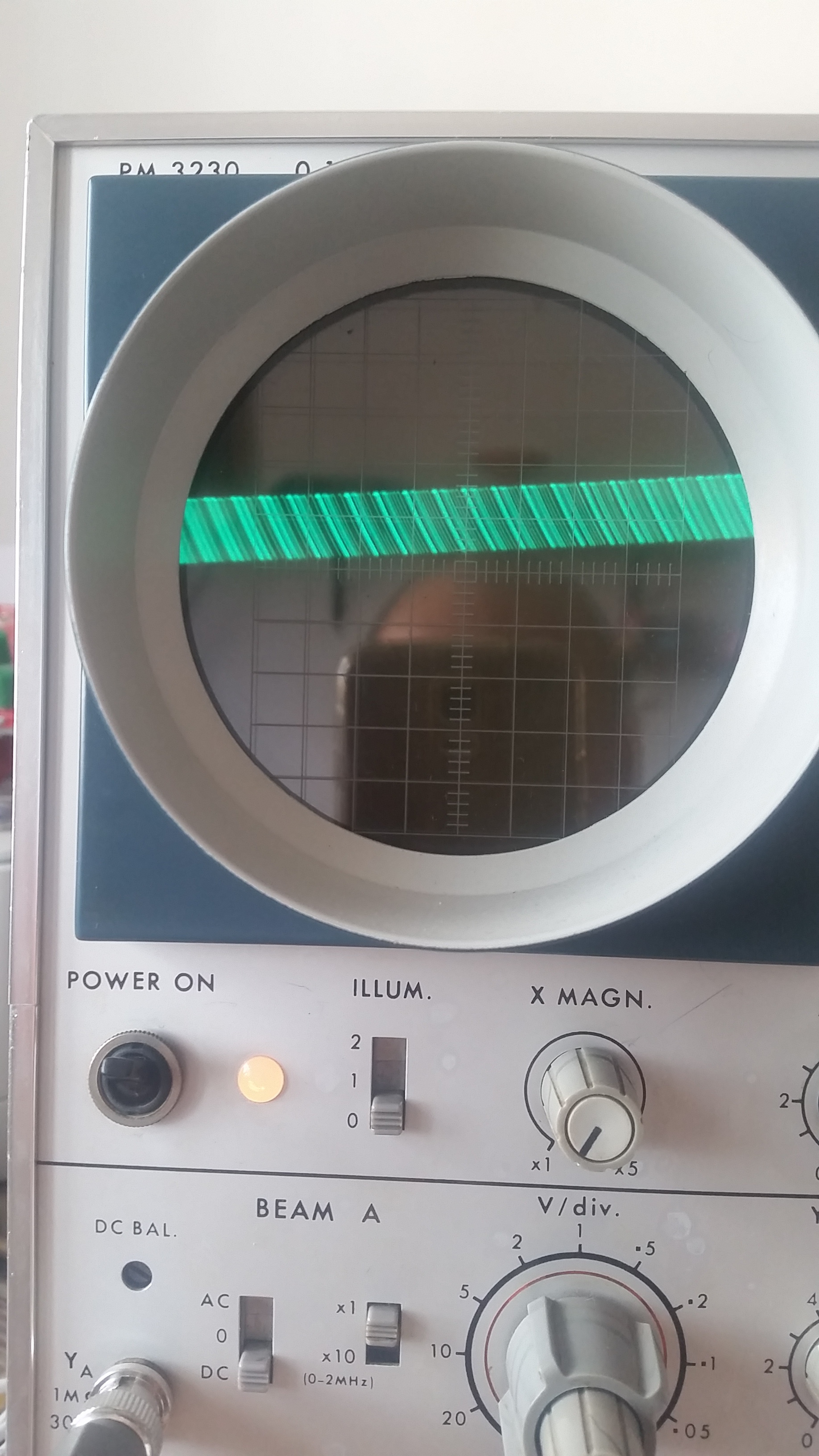
OK Gents, unfortunately that was not enough. But, I now get some signals
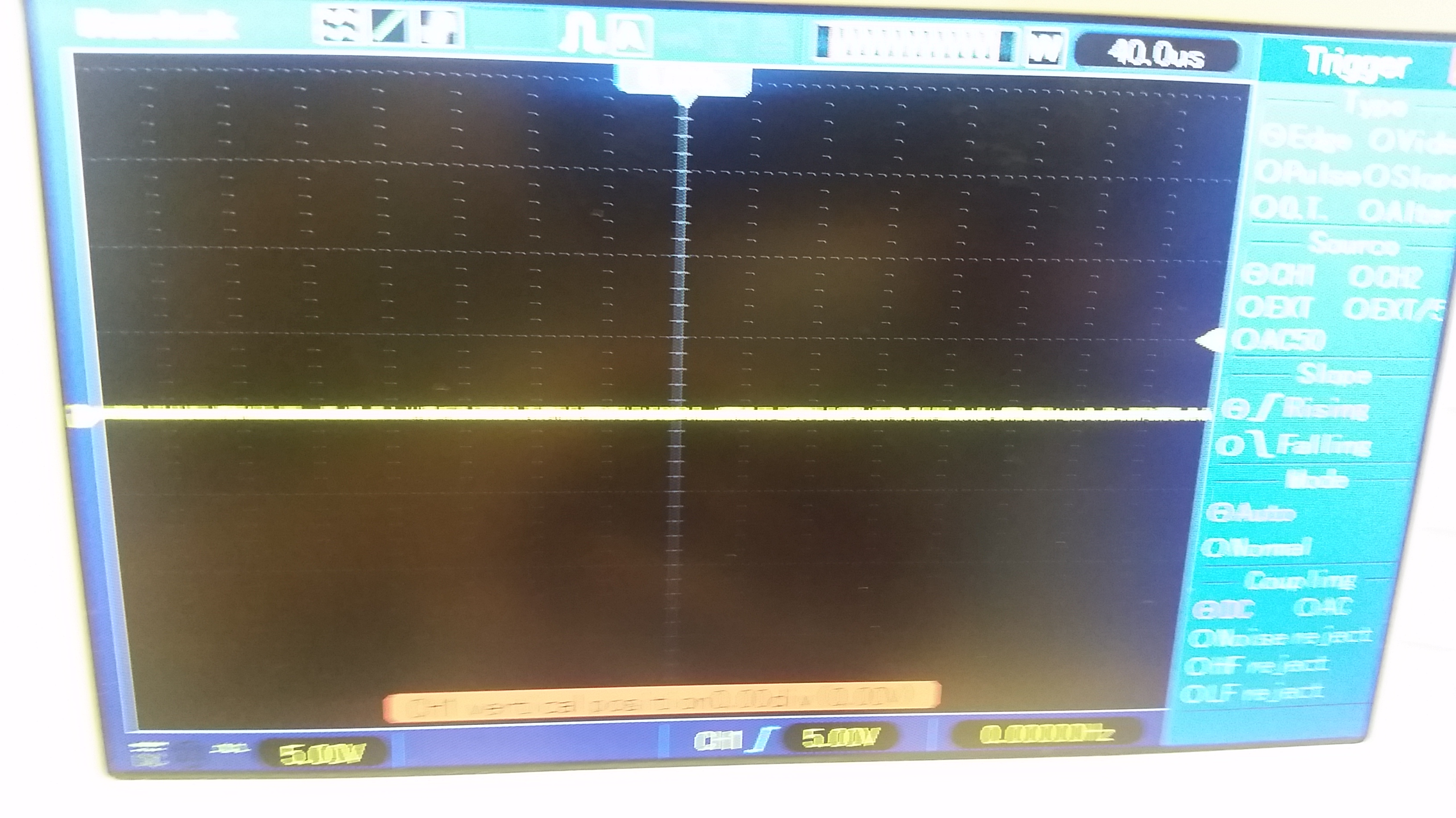
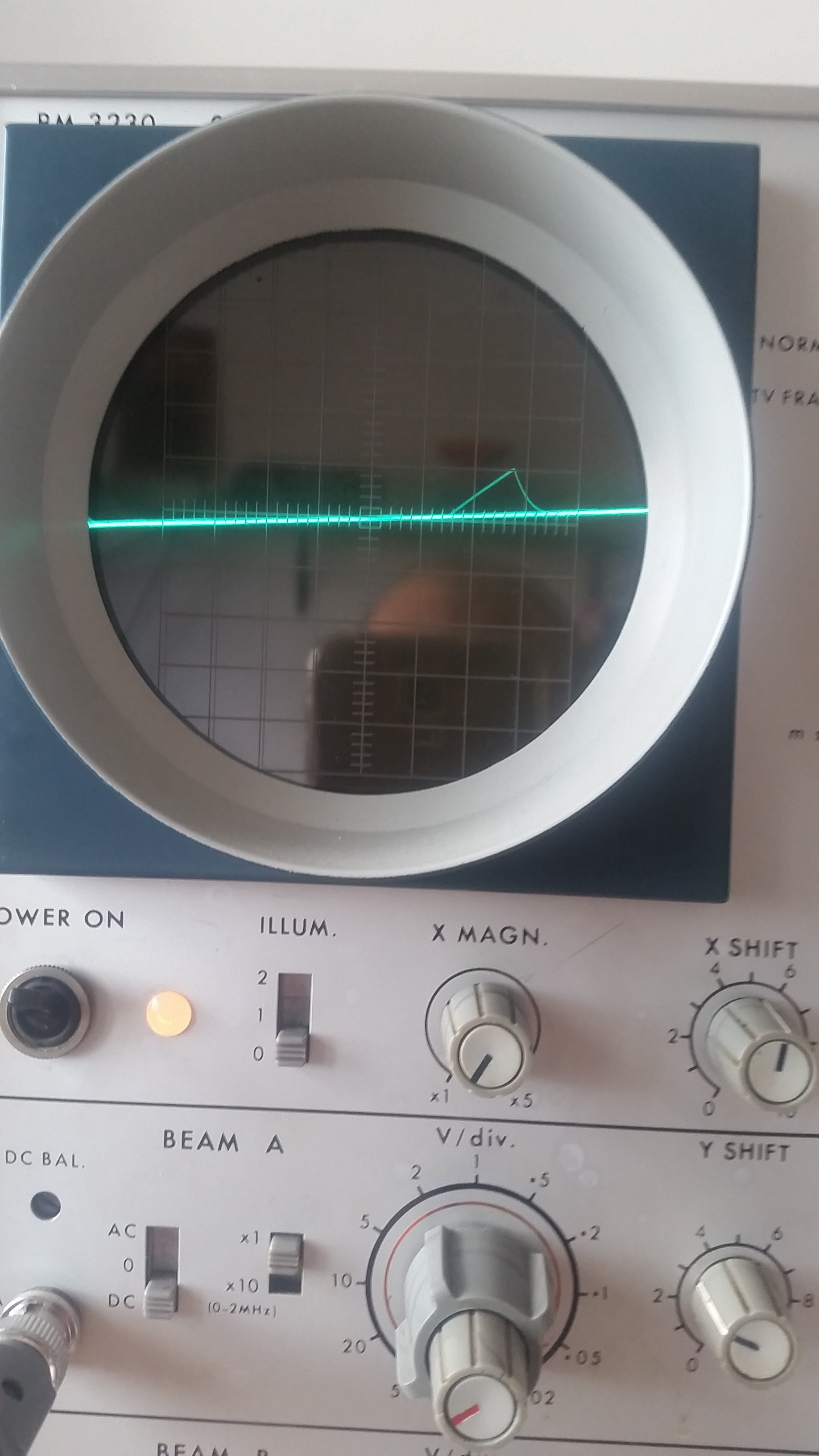
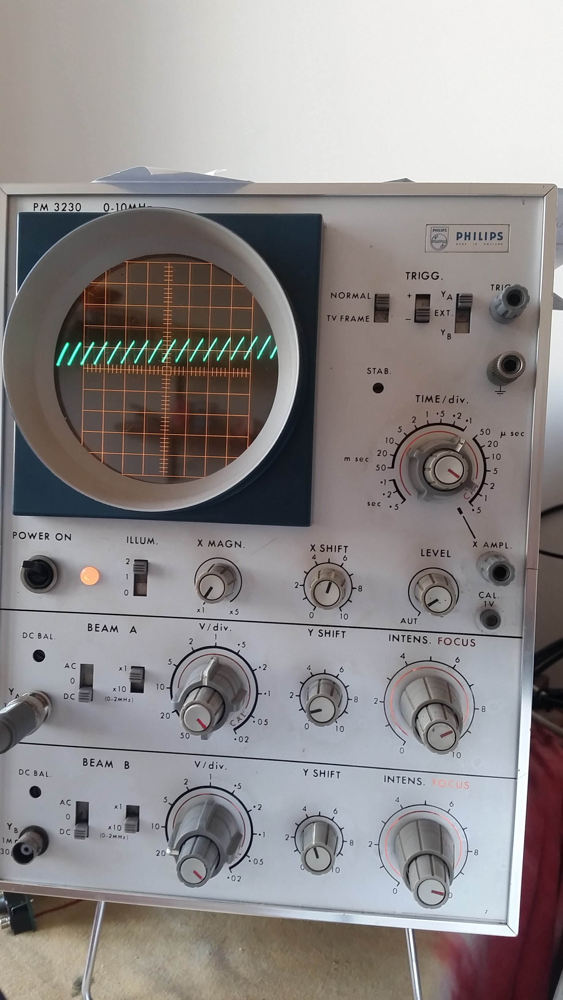
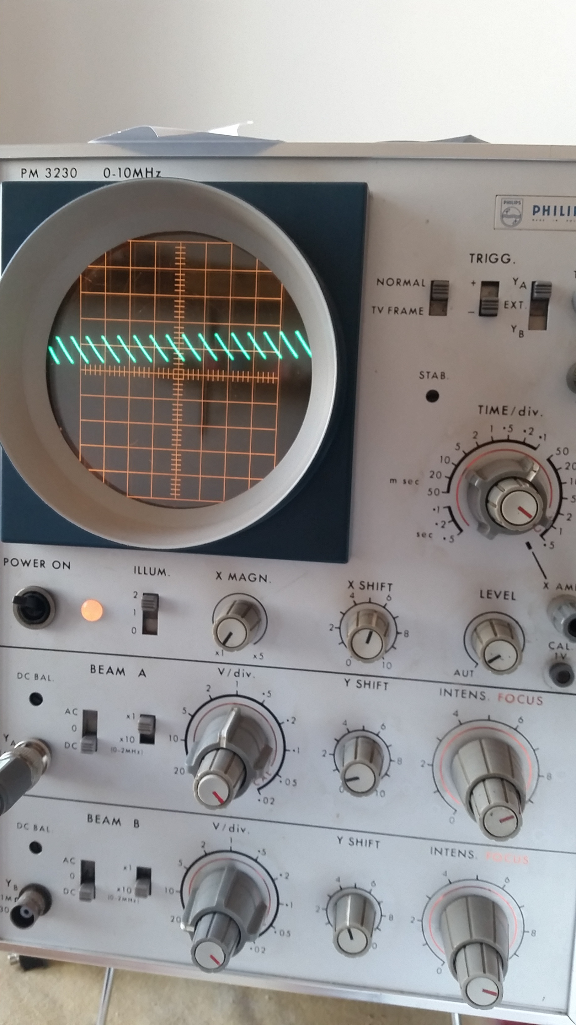
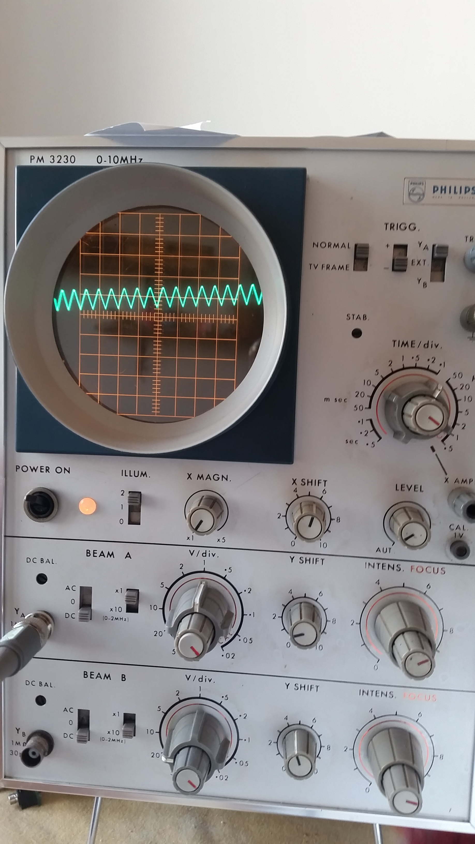
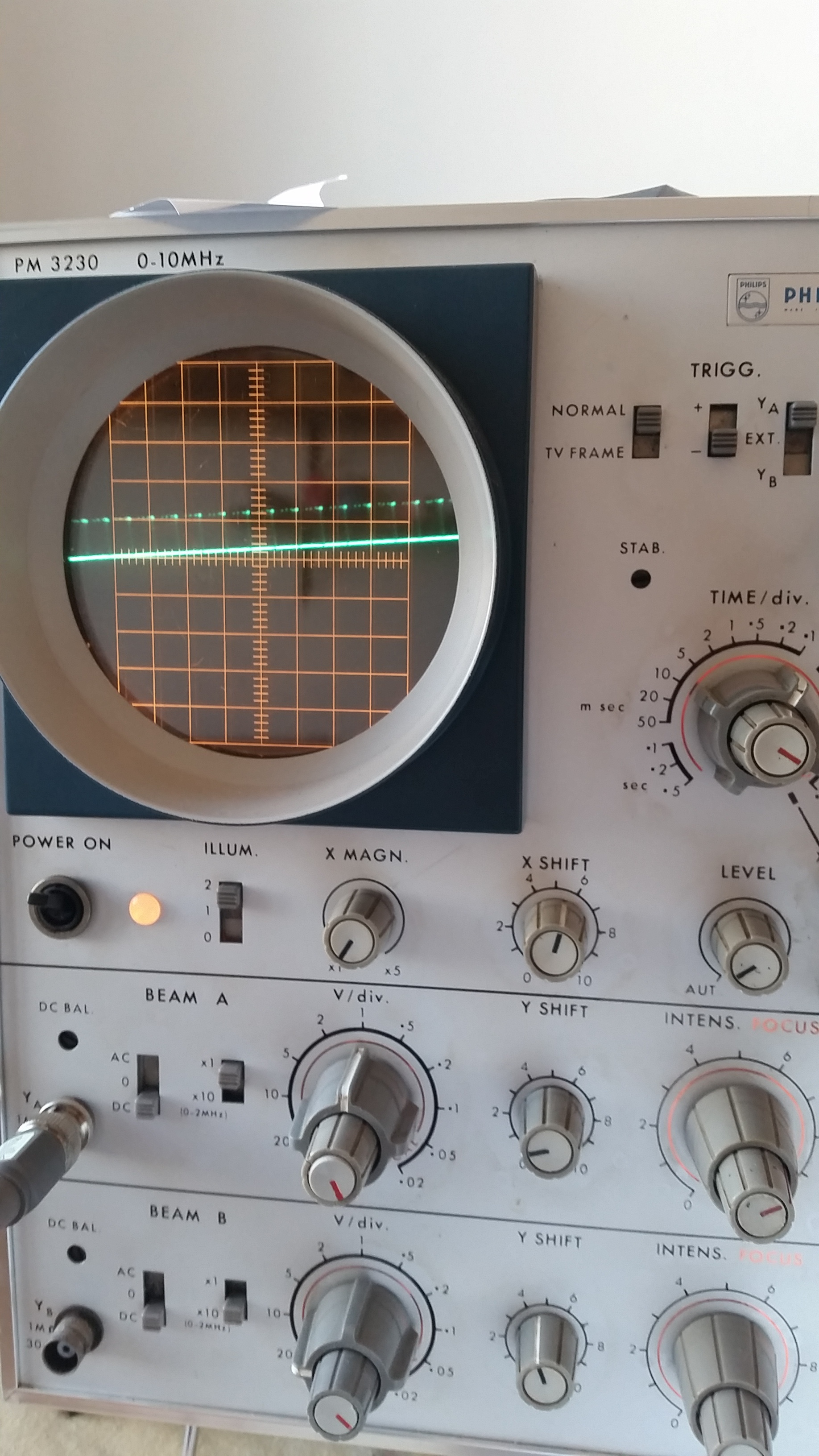
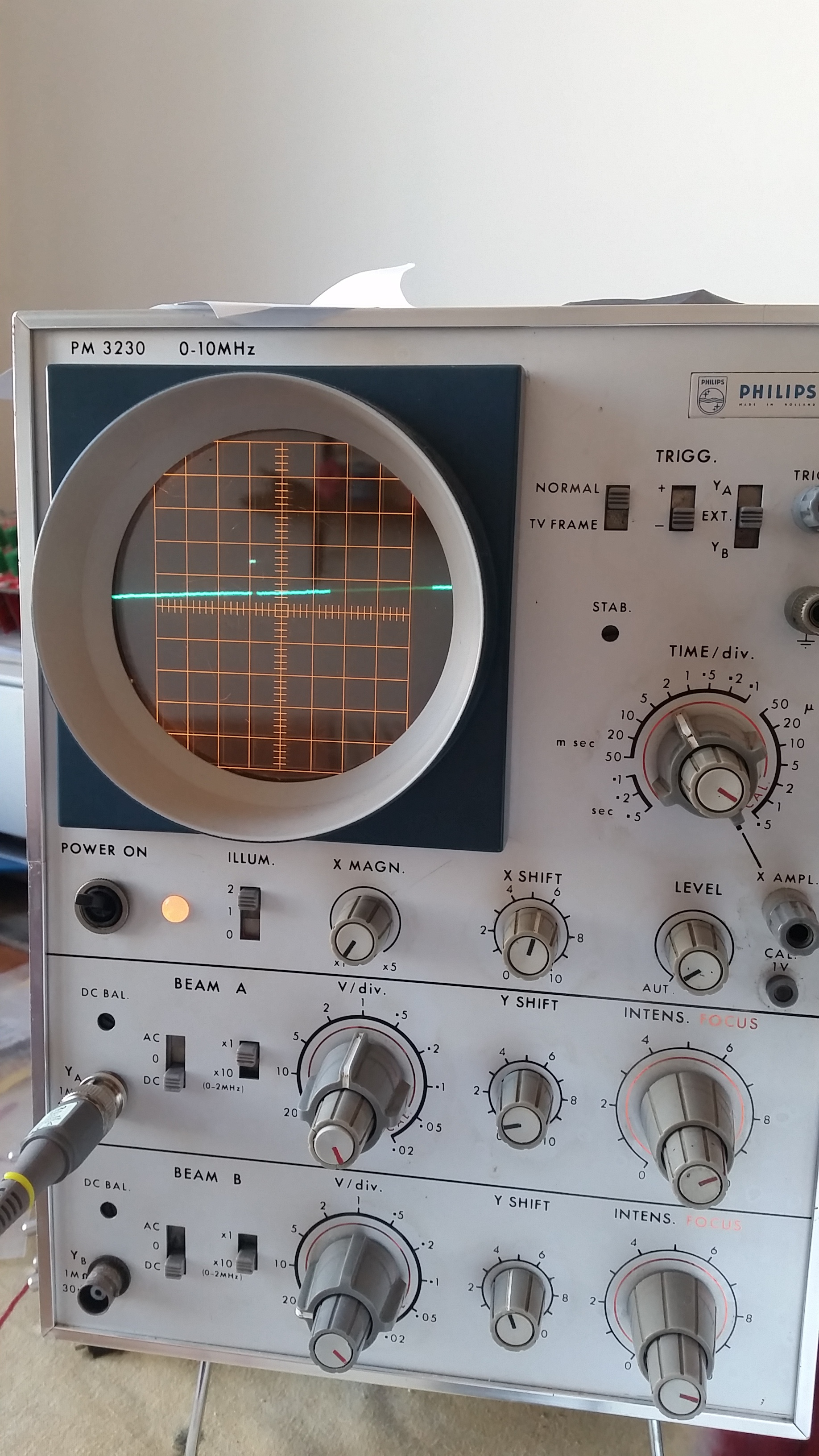
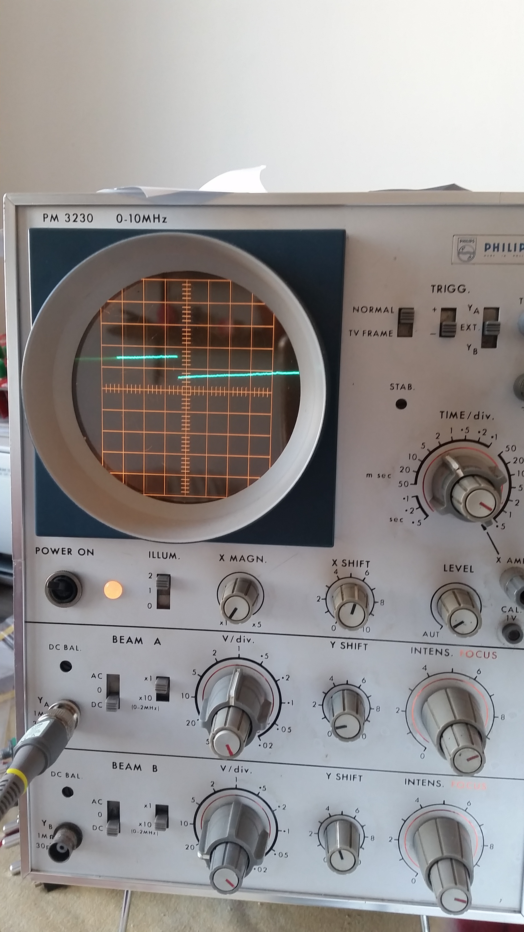
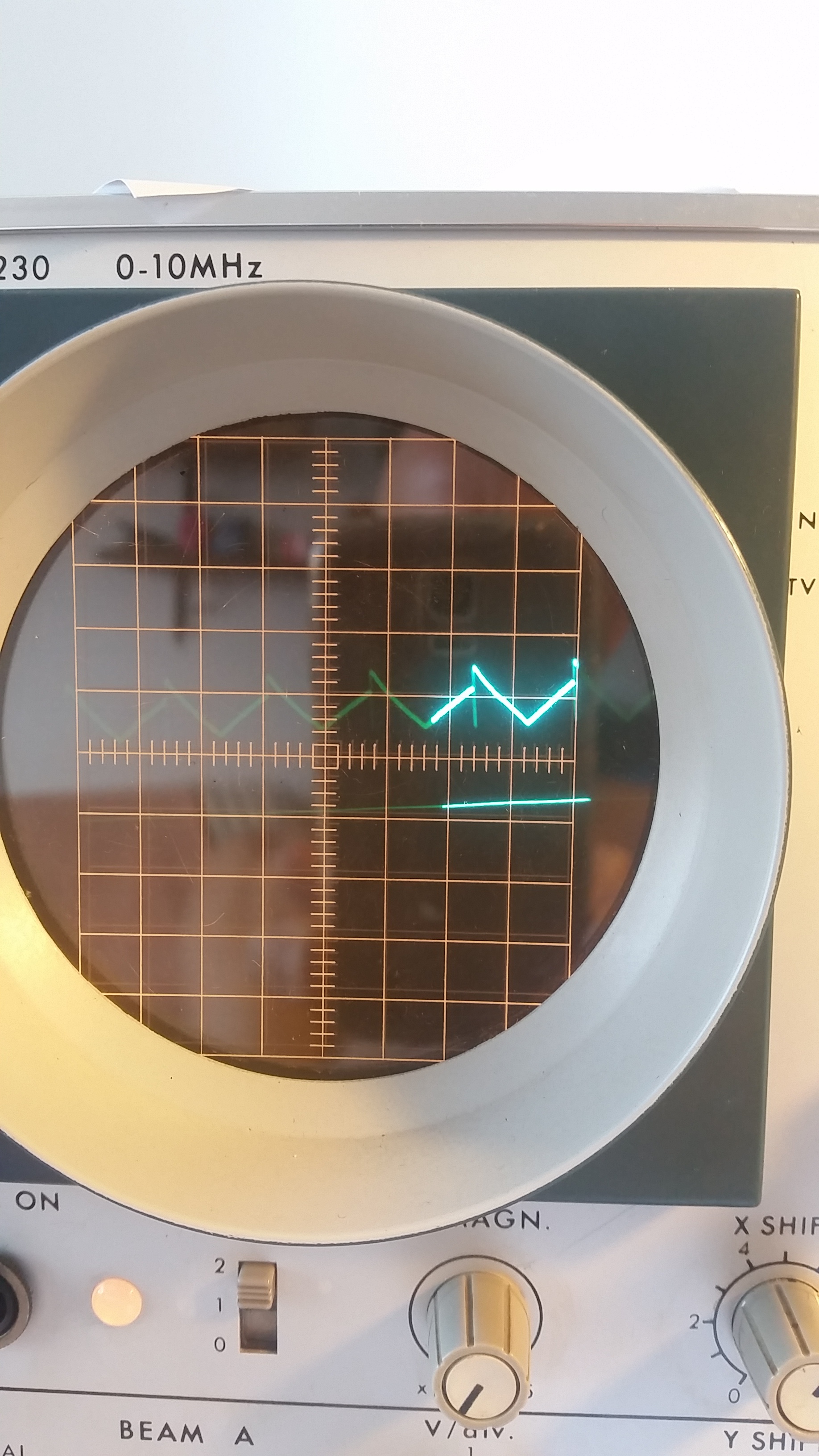
I see some ramps, that are very weak (around 200mV I think). The trimmer makes them bigger but that’s the max I reach. It seems they are freq modulated
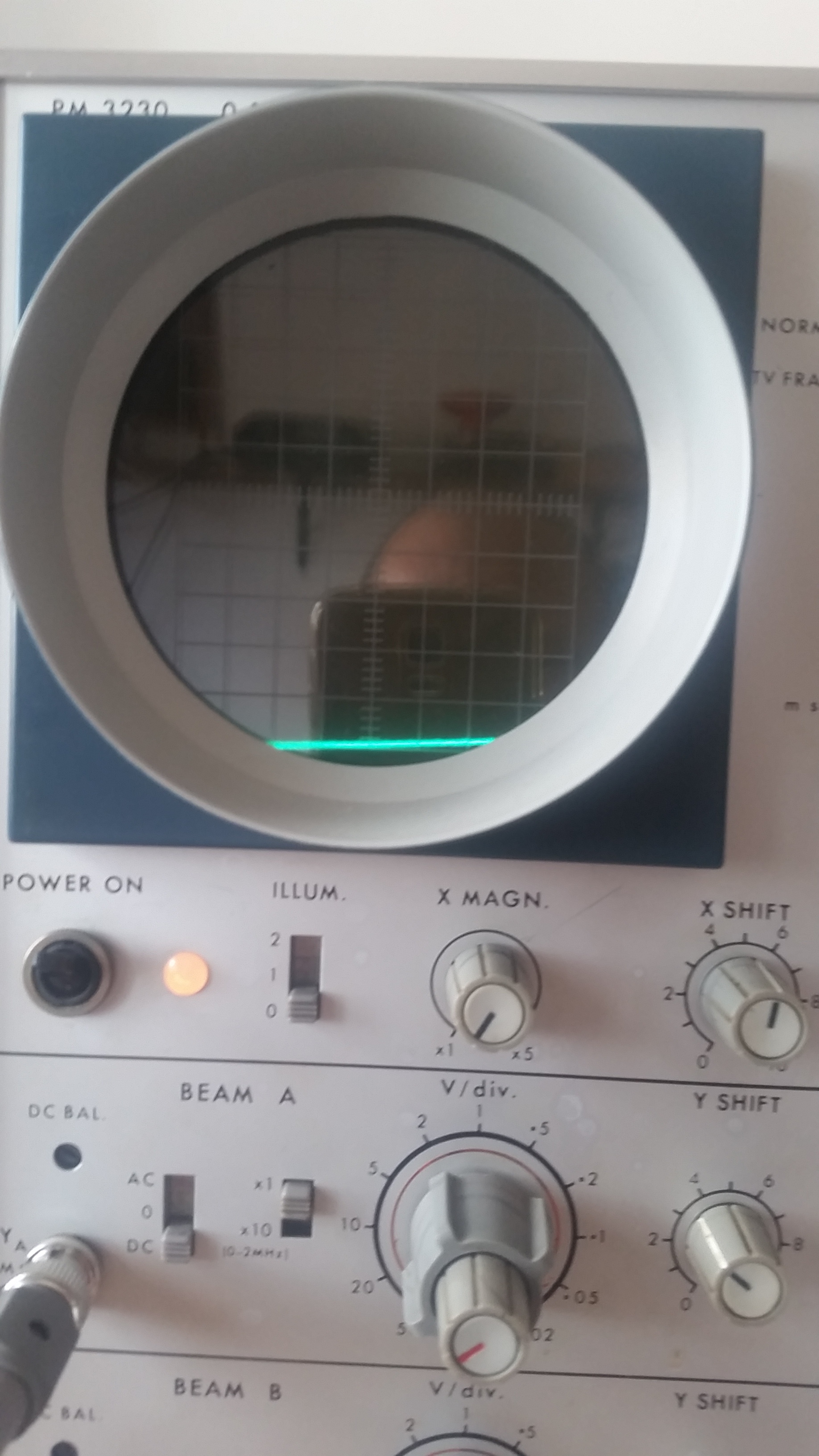
I can’t stabilize them with my old scope. I show you some pictures of the six outputs ! Sorry for the quality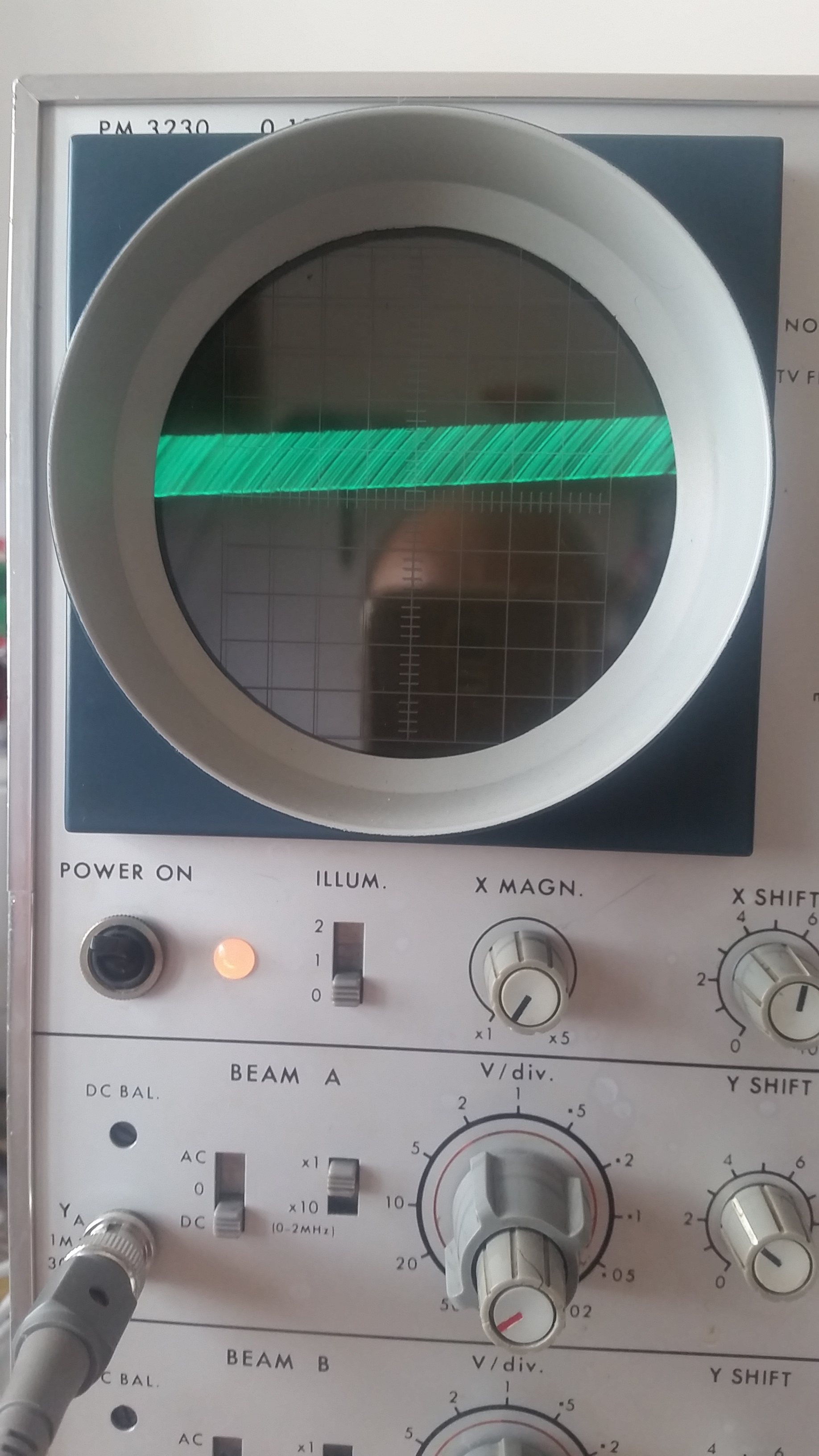
#15 — VisibleSignals · 2020-09-02
It would be an interesting coincidence if both signals were at the lower level, since they don’t really share any circuitry other than the power supply. Can you make sure you are connecting Ground when you’re making your readings?
Viewing video on a 10MHz bandwidth scope is pushing it near to its limit, so those images are pretty good really. Here’s the scope’s manual: http://bama.edebris.com/download/philips/pm3230/PM3230%20manual.pdf
You may get more stable results connecting the source video signal (that you are inputting to the Cadet I sync gen) to the trigger input in the top right corner, and selecting TV Frame. The smaller outer knob on the V/div adjusts how many volts each division (i.e. between the lines on the scope’s screen) covers, and on most scopes I’ve used it would normally be set all the way to the right for calibrated use. I can’t be sure if that’s true for this scope since my Dutch isn’t good enough
If it turns out the ramp voltages really are attenuated then start by check the U12.2/U13.2 output voltage on the scope - it should go from 0V to 1V.
#16 — Fox · 2020-09-02
What kind of probes do you have too?
#17 — jestern · 2020-09-03
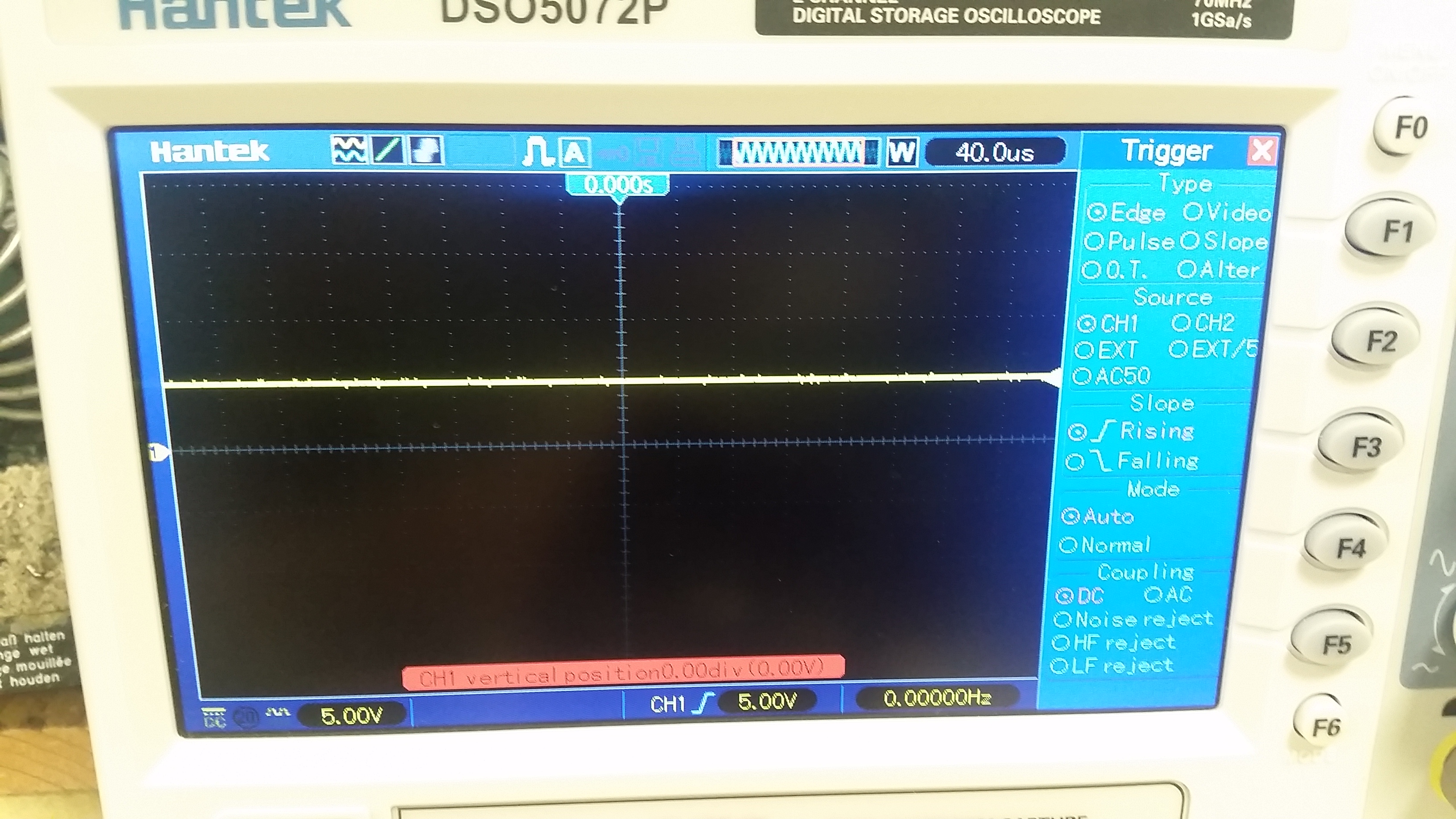
Hey thanks for your help and quick answers. I just found out maybe the probes were set on attenuation 10 !!! Ok so I’ll try to get my shit together with scope and probes and come back with more reasonable results / measurements
I really appreciate all your help !!!
#18 — VisibleSignals · 2020-09-03
That’s great news! Nothing beats finding a simple problem. I’m sure you’re very close!
#19 — jestern · 2020-09-06
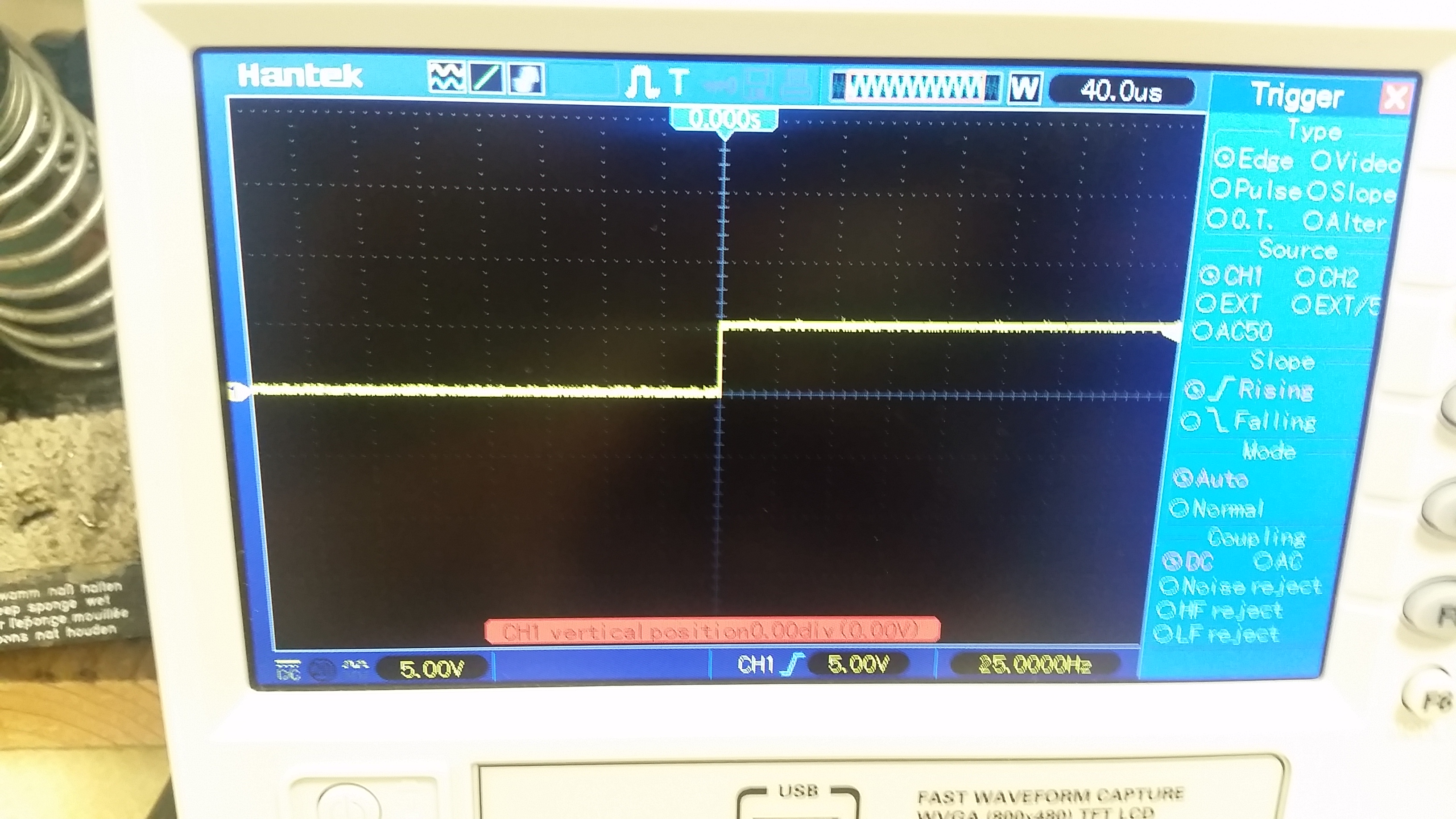
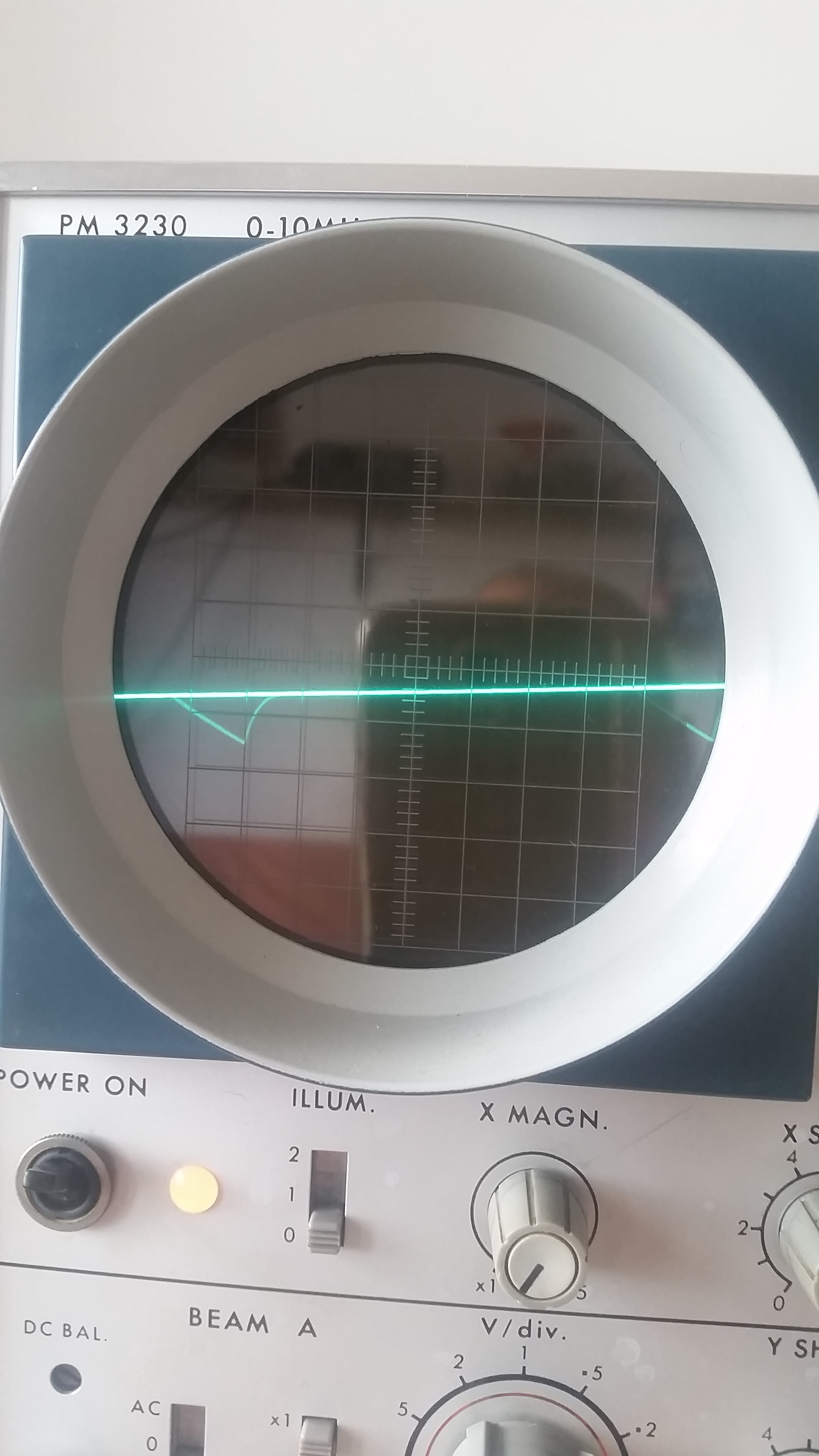
Ok I’m here again now the Horizontal part seems to work fine. I had a burned IC. But the Vertical is still off. I suspect it is in the Sync Generator.
Here the horizontal:
My Sync Generator outputs these three signals from the jacks:
The Horizontal Sync signal reaching the Ramps module seems logical while the Vertical Sync is very weird having spikes that I can’t stabilise in time. Is it supposed to be the same that comes through the jacks? I’ll keep on checking. The ramps seems ok to me I checked for shorts, power for the ICs, changed the ICs checked resistors being symmetrical between horizontal and vertical.
#20 — Fox · 2020-09-06
Those ramps look great!
Vsync should be far slower and wider than Hsync, so it should be easier to capture on your scope. Intermittent spikes may be related to a floating input or no negative feedback or maybe even something else.
On to the cadet I schematic, we see that the output opamp is shared between both sync signals: U1.
For starters can you disconnect the other modules form Cadet I and probe the two signals? Please then measure the resistance and continuity points of R3 (3.92K), R6 (1K), R14(1K), R5(499R) and R20(499R).
If these seem accurate, swap U1 with another op amp and look at the signals again.
#21 — jestern · 2020-09-06
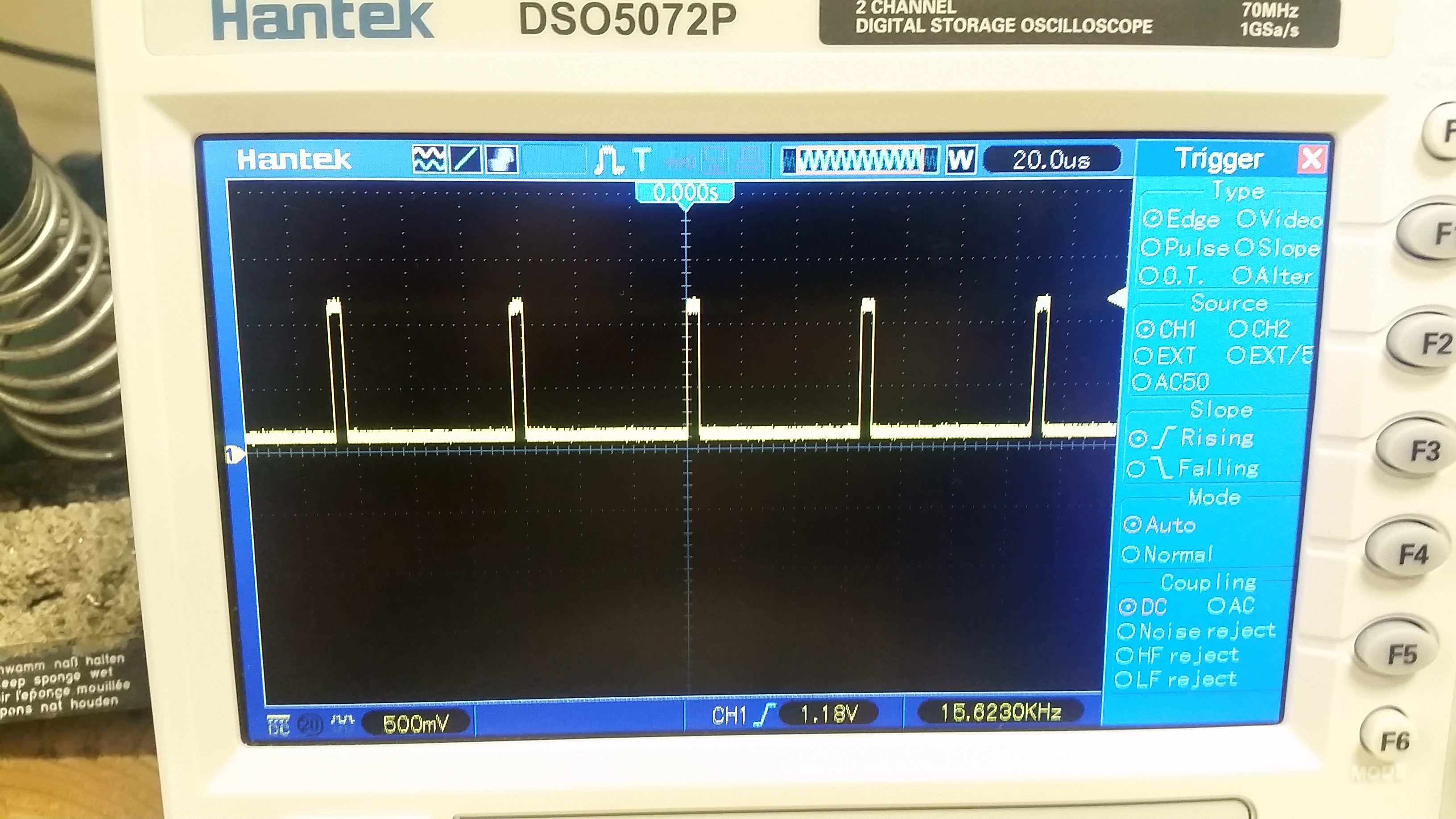
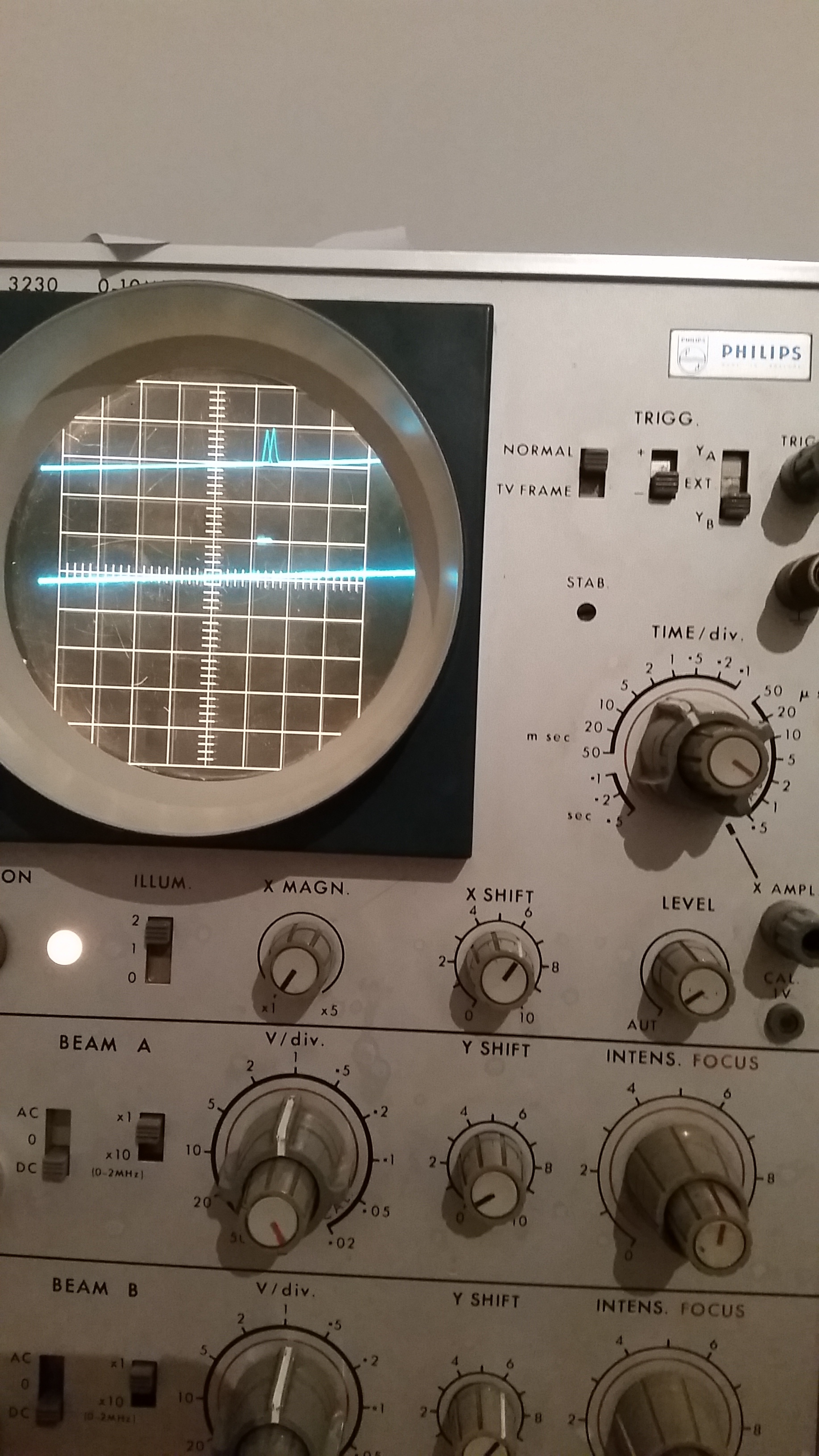
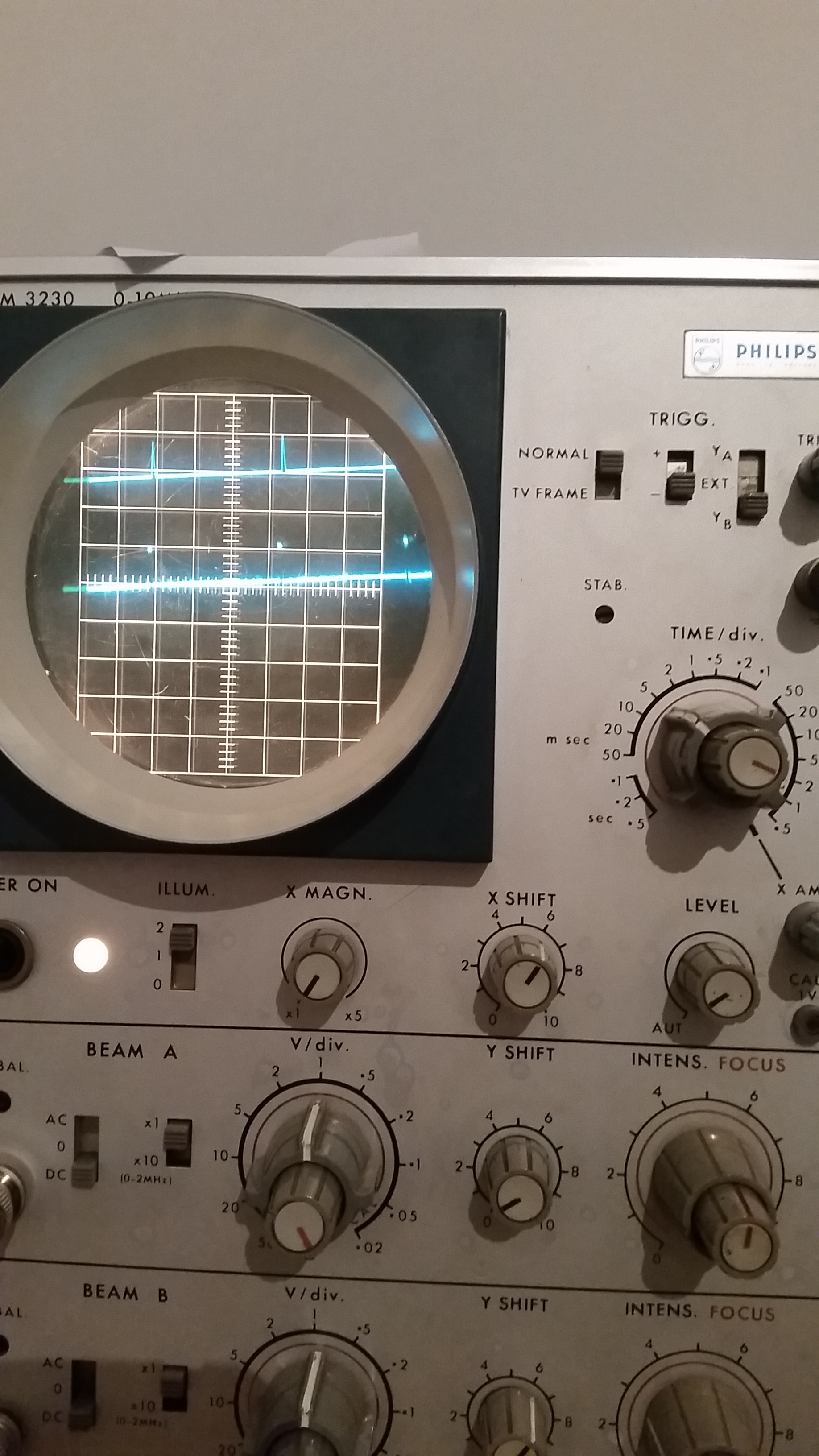
ok so I checked the Sync Gen and it seems ok. I don’t see continuity between the output of R20 and any of the pins of the syncplug. BUT if I look at R27 on the Cadet Ramps I see a signal (with same amplitude on both extremities of R27 which seems strange to me) identical to the Vsync jack out of the SyncGen: it has think spikes at same frequency only at R27 they are 5V of amplitude while on the output of SyncGen they are at 1V. Estimated spacing 15 msec. Switching NTSC to PAL in the SyncGen doesn’t seem to change anything, which is also strange.
I tried changing the opamp and it does the same.
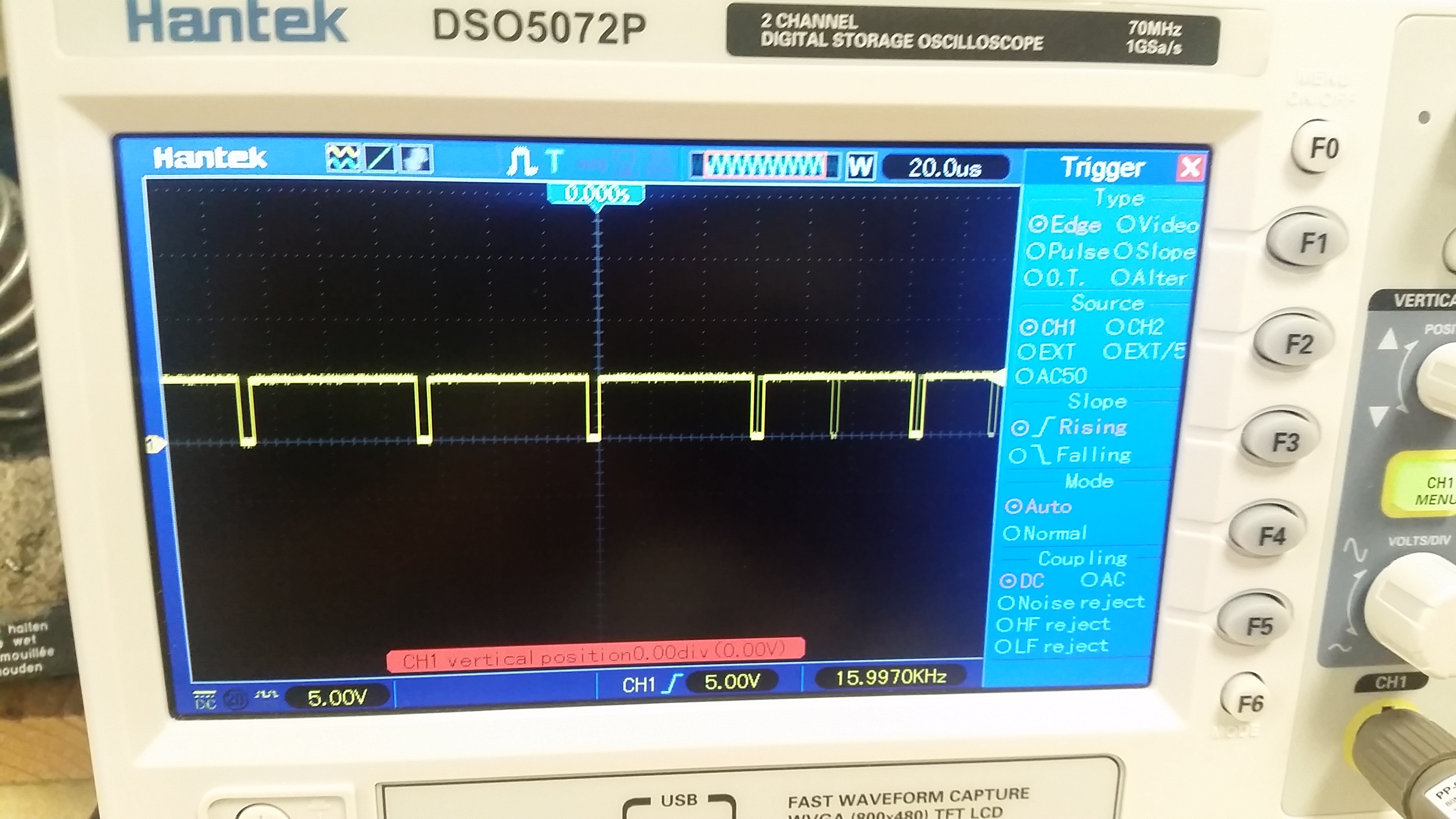
Strange thing is: after pluging and repluggin sometimes I see in the V output of the Ramps some little ramps (not long but quick, check the pictures) sometimes nothing. I think my SyncGen could be fine. Don’t know what could be wrong then. I have a dual scope so in the picture you see the sync signal from the SyncGen (below) and the V Ramps (above). Only difference the time scale. Maybe the cap is too fast in releasing the ramp? I dont know what I’m talking about but that’s the only difference in both circuits H and V.
#22 — Fox · 2020-09-06
The voltage range going into U7 on the ramps board should be 0-1v and the output should be 0-5v. The op amp may be good then.
I wonder if the connection between R20 (CADET I) and U7 (CADET IV) is broken. That could point to either 14-pin connector or even the 14-pin cable itself.
If the input of an inverter (U7) is left floating, it will probably self oscillate at the output so if R20 does not connect to U7, then the inherent capacitance of the traces and cabling would determine a specific frequency of self oscillation (for example 15mSec).
I think you should investigate here:
I don’t see continuity between the output of R20 and any of the pins of the syncplug.
EDIT: Oops, I said 14-pin connectors and ribbon cable. But R20 should go to the 16-pin cable.
#23 — jestern · 2020-09-06
Hey Fox thanks!!! My problem is I don’t know to which pin it should be connected to. I don’t see it even of the same board of the SyncGen. I just see the same frequency in the jack out and the sync in to the Ramps so I would think it can’t be self oscillation. But then again I don’t know much. Maybe there is a sort of resistance that is non 0 between r20 and the pin of the sync plug…
#24 — Fox · 2020-09-06
I edited my post above to say that I meant 16-pin ribbon cable and not 14-pin ribbon cable.
R20 must connect to the GATE pin on your 16-pin power ribbon.
#25 — Fox · 2020-09-06
Jeez, I just put the schematics side-by-side again and Ramps doesn’t use the signal from R20. It DOES use the signal from pin 9 on the 14-pin ribbon cable. Tracing that back, the signal goes to U7 on CADET I which in turn gets the v/hsync signals directly out of the Atmega.
Backing up, I know you replaced Q2 on your ramps board, but didn’t say if you had looked at Q1. Both Q1 and Q2 are supposed to be 2n3906. Just to be clear.
#26 — jestern · 2020-09-07
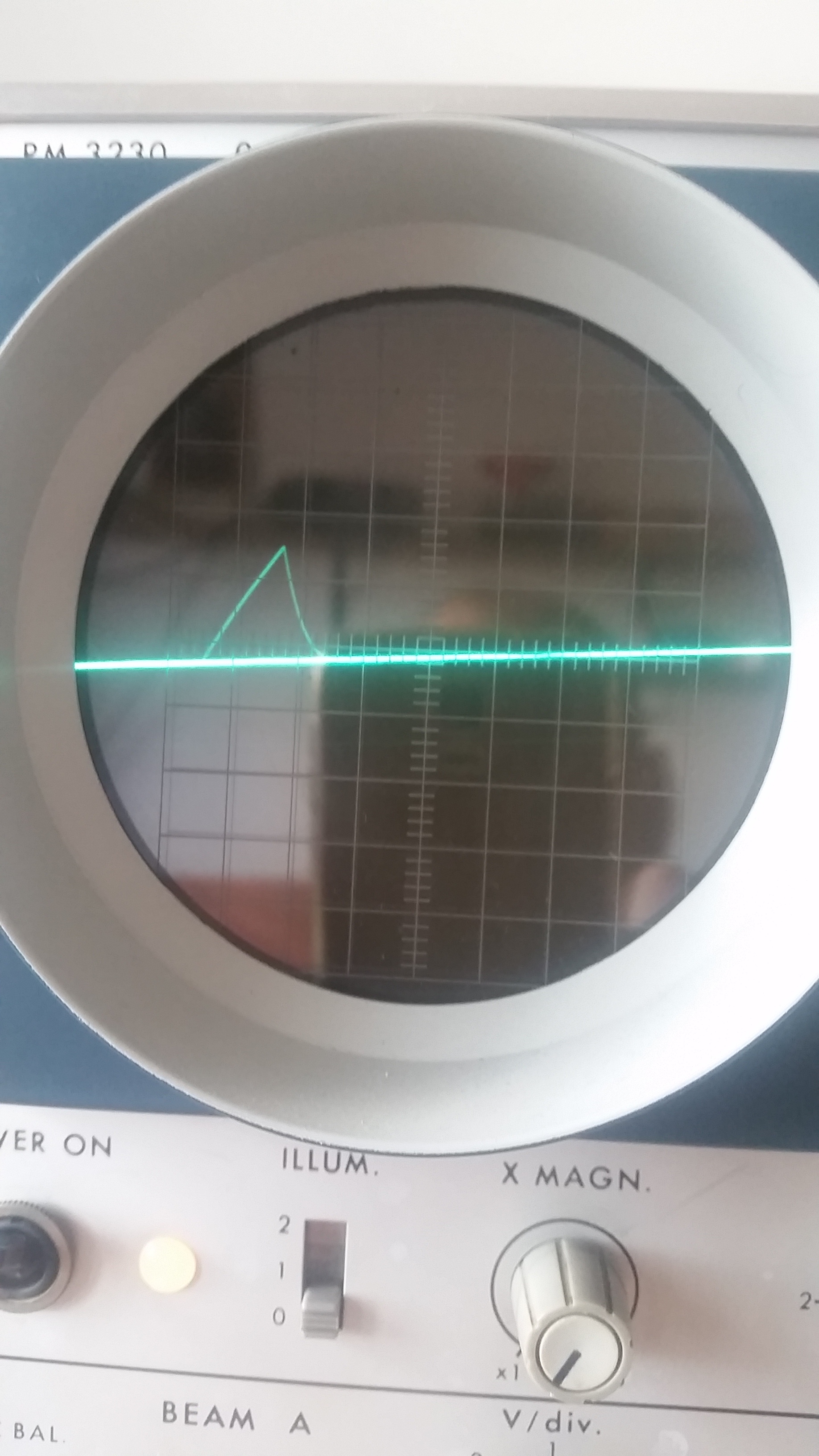
Thanks so much Fox I think I found it there was a broken trace somehow. Now it all works almost fine. I just have not the best looking ramp in
the H triangle. Here is the picture. Moving the trimpot it feels like I just need more resistance to make that central bump disappear. What do you guys suggest can I add a bigger resistor in place of R4? Which value would you say? Like 10k?
Thanks so much really for the help!!! I’m almost there!!! :))))
#27 — Fox · 2020-09-07
No, R4 won’t fix it. R4 is for the V-sync portion anyhow…uh, correct me if I’m wrong. Maybe you meant R2.
This looks like a symmetry issue with the Triangle shaper portion. Can you verify resistor values, solder continuity and diode polarity of this portion:
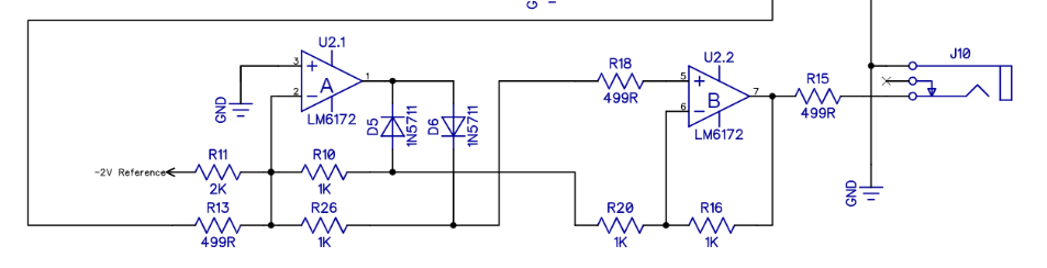
I suspect R10 and R26 must be very close in value to achieve that shape we need. Of course, R18 and R20 are just as important here. My reasoning is that one side if the triangle is being attenuated at a different amplitude than the other side; each side being technically the same triangle, but inverted and non-inverted versions summed together through the diodes.
#28 — jestern · 2020-09-07
HI Fox, thanks a lot for the wisdom. I checked the color codes and they are ok, diodes and continuity. All resistors are 1%. I can also run a value check tomorrow. Anyway whenever I turn the trimpot I see also the other two curves not reaching their optimal point. That’s why I thought the problem was that I need more resistor in my trimpot. In my Horizontal trimpot I am using the max position and I luckily to get perfectly where I want. So maybe it’s just my whole values don’t add up as expected and need to tweak a resistor somehow before or after the trimpot.
#29 — Fox · 2020-09-07
The trimpot/R2 combo can only attenuate the signal since both sides of it are buffers. R2 sets the low limit of possible attenuation while the high end is 1:1(no attenuation). This isn’t a gain stage, but it sounds like you want gain.
Theres also the possibility that the capacitor (C29) is not charging to a high enough voltage within the time of one Hsync. I’m not sure which resistor fits into the RC equation, but even the value of C29 would affect the rate too. But It would probably have to be off by more than 10% to see a difference.
I am not certain enough of this part to offer any suggestions. Maybe someone else will chime in with a better solution.
I looked at your color codes too and everything seems to be right, at least visually.
#30 — jestern · 2020-09-07
thanks in the meantime I’ll check the values of the resistors to see if there is one off. solved most of my issues anyway
This is a great community <3 Maybe I’ll wait a week and in case I’ll ask again on Facebook.
#31 — VisibleSignals · 2020-09-08
The circuit section that Fox posted is a Full Wave Rectifier - it works by taking a bipolar signal and inverting half of it. By doing so it gives the fade from 1V to 0V back to 1V across/down the screen.
The trimpot adjusts the amplitude of the ramp output from the oscillator core U12.2. You want that waveform to be a 0V to 1V ramp from one edge of the screen to the other, so it can be buffered to J8 via U12.3. The rectifier circuit doubles that input signal to 0V~2V (R13:R26 ratio is 2:1) and adds half of the -2V reference as an offset (R11:R10 ratio is 1:2). So the -IN to U2.1 is a ramp from -1V to +1V. The rectifier inverts the negative portion of that wave, resulting in a 1V to 0V to 1V waveform. Got all that?
So, if the trimpot is adjusted then the waveform has more or less voltage above the (effective) 0.5V threshold around which it is mirrored to form the V shape. So yes, changing the trimpot should adjust the symmetry of the V shape. If you’re at the extremes of the trimmer than you could reduce R2 to allow you to reduce the amplitude of the wave, but to increase the amplitude it’s not so easy, since the non-inverting op-amp feedback resistors of U12.2 U12.3 are currently zero, restricting you to unity gain (see https://www.electronics-tutorials.ws/opamp/opamp_3.html for more information about that). But reducing R44 slightly should result in higher current flow into C29, resulting in a faster charge and therefore a higher potential (i.e. voltage) before the reset happens.In response to some of Fox’s points then:
- R10 and R26 are important, but only in relation to R11 and R13 as they set the relative thresholds for the mixing of the (scaled) -2V reference and the main ramp signal and therefore control the rectification point.
- R10, R26, R20 and R16 must all match, or else the ‘angles’ of portions of the rectified waveform get skewed.
- R18 is actually not important at all, and could probably be replaced by a wire link!
Jester, check the voltage of the -2V reference, and make sure it’s correct. Replacing R11 with a 2.5K trimpot (wired as a rheostat) would allow you to adjust the rectification point independent of the amplitude of the other outputs, but that really shouldn’t be necessary if all of the resistors mentioned above are correct.
Sorry for the complicated description - I probably need to draw a diagram of the waves at various points! The take-away here is simple, though: Lars is smart
#32 — Fox · 2020-09-08
@VisibleSignals Excellent description and suggestions. I completely overlooked the -2v reference because the Vsync triangle looks good, but adjusting R11 will change the “fold point” of the Hramp and could make the H triangle symmetrical again without affecting the V-outputs!
I see now how the H-ADJ trimpot and R2 could change the shape of the H triangle too.
@jestern, As for the vertical line down the center of your two ramps, this is a common side effect of rectifiers and should not be visible on your tv. If you zoom in far enough on the V ramp, you’ll likely see it there too.
#33 — jestern · 2020-09-08
VisibleSignals wrote:
R10, R26, R20 and R16 must all match, or else the ‘angles’ of portions of the rectified waveform get skewed.
Thanks guys I understood more or less I’ll check the values of R10, R26, R20 and R16 first then in case replace R11. I’ll ask if I have doubts !!! Almost there I feel.
#34 — jestern · 2020-10-09
Ok guys I solved it I have now a working Ramps. There is still a little bump in the middle of the triangular wave but it seems acceptable in the image. I think my old scope was driving me insane and I could not see what I was looking for possibly it was working when I left few weeks ago. Anyway now it’s solved. The problem now is the input from my Extron but I’ll ask it in another thread thanks so much <3 <3 <3
#35 — VisibleSignals · 2020-10-09
Great news!
This sentence is padding to get my post length to 20 characters.