[ORDER] dual A+B-C & dual Rectifier
Category: Unknown · Tags: — · Posts: 5
#1 — Fox · 2021-09-09
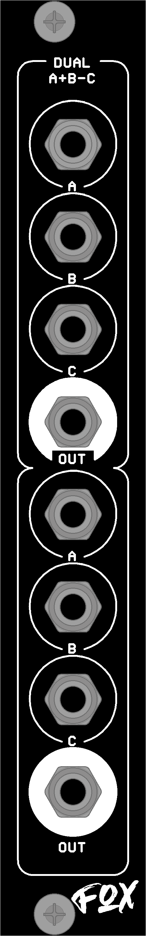
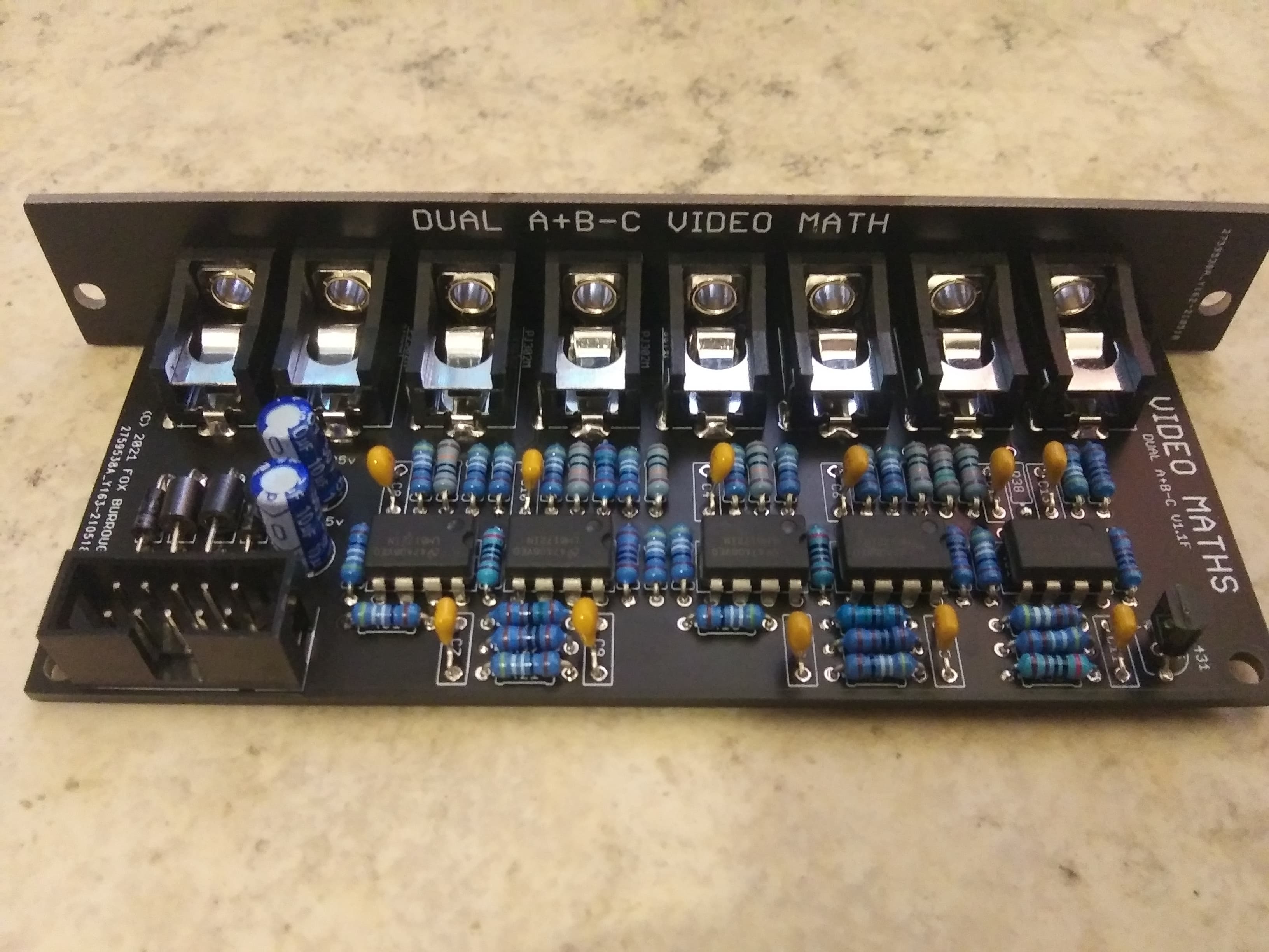
A+B-C offers two 3-input mixers, each with two positive inputs and one negative input. Perform simple to complex additive and subtractive mixing with video signals.
Alternate fixed mixing configurations can be made at build time including:
- A+B-C
- (A+B)/2-C
- (A+B-C)/2
The “A+B-C” configuration means that your first two inputs will get you closer to white and your third input will bring you closer to black. This will give you the most stark results possible with this mixer.
The “(A+B)/2-C” config adds your first two inputs together and then halves the output so it is unlikely your mix will blow out to white. Then you can subtract (or bring closer to black) the whole mix with another input. This gives more of an ‘averaged’ look, depending on what you feed into the C input.
The “(A+B-C)/2” config is the same as the first configuration but it halves your output (making white → mid-grey). This makes it much less likely to blow to white than the other two combinations and will generally give you darker outputs.
The A-input of the first section is normalled to 1V (white) so you can perform simple subtractive mixing with an image if you don’t patch anything into A or B.
The first section’s output is normalled into the second section’s A input in all configurations. Plug 5 sources into section 1’s A, B, C and section 2’s B and C to get a complex mix in any build config!
- 4 HP
- 47mm deep
- 31 mA +12V
- 27 mA -12V
- ModularGrid
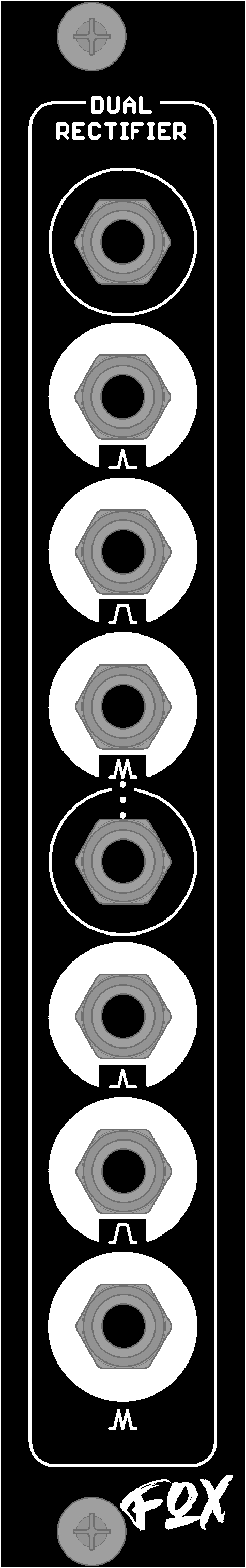
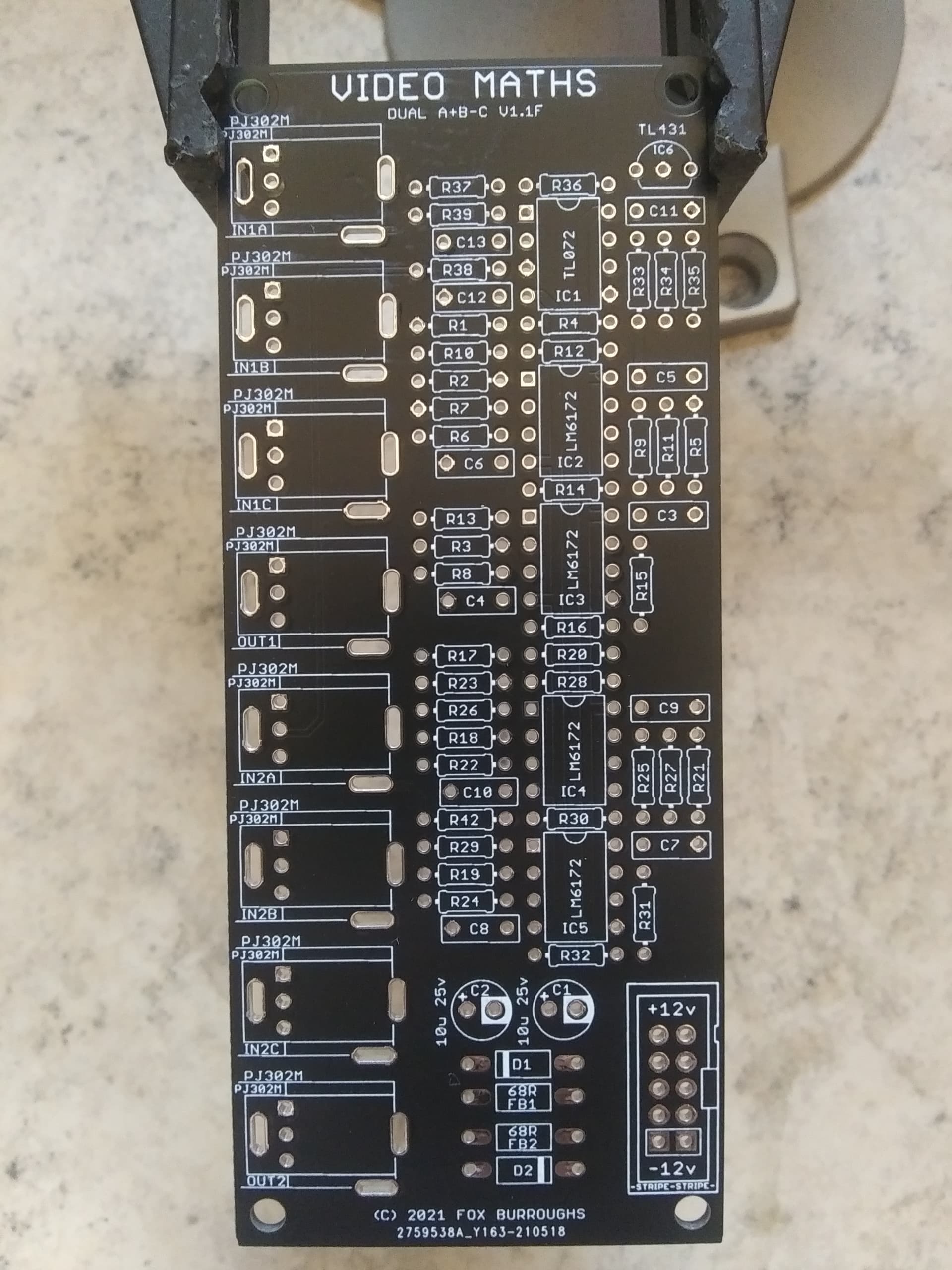
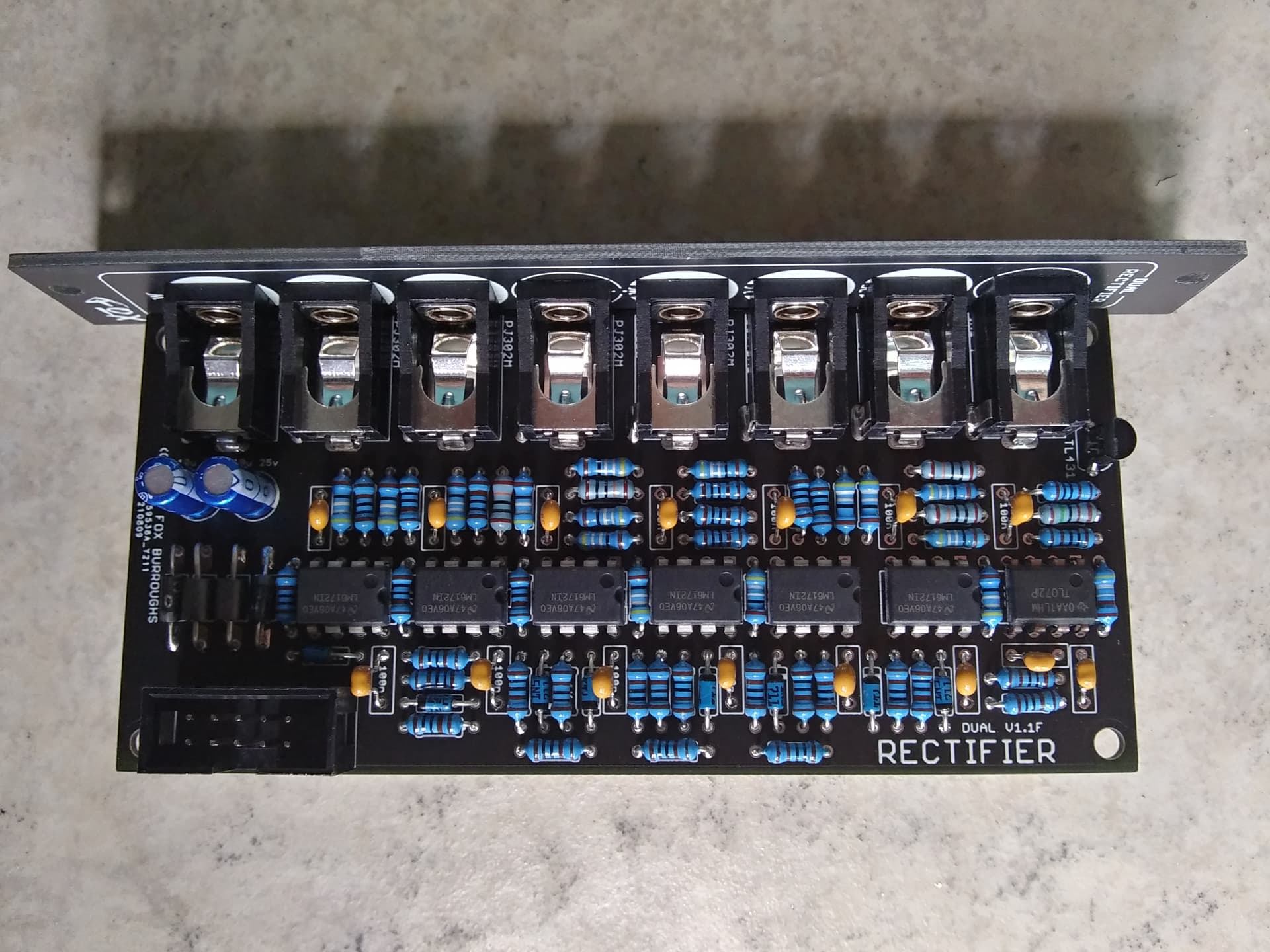
Dual RECTIFIER offers two clipping and frequency doubling sections.
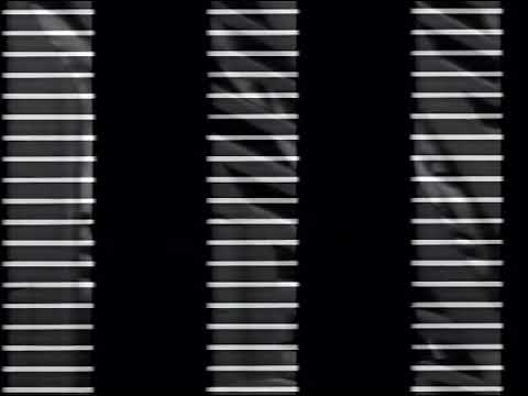
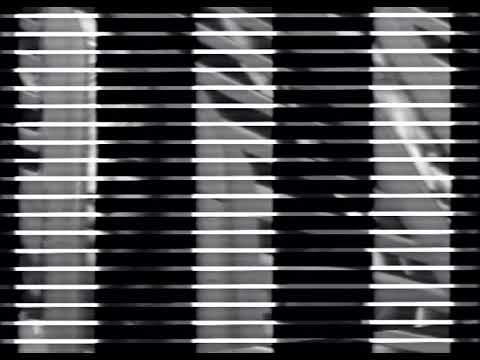
The first output clips inputs below mid-grey and accentuates the bright portions of the signal. The second output clips signals below mid-grey and accentuates the darker portions of the signal. The third output gives a single stage solarization or frequency doubling effect.
The third output of the first section is normalled into the section input’s section for more variations of one signal. Putting a signal into the top input and taking the bottom output will give you a twice frequency doubled output.
- 4 HP
- 53 mm deep
- 41 mA +12V
- 38 mA -12V
- ModularGrid
Prices:
DIY PCB/PanelBuiltA+B-C$22$131RECTIFIER$22$145 See other available modulesDIY PCB/PanelBuiltMULTA$16$87MULTB$19$104SHUTTER$32$163VEIL$28$157Passive Switch$10naSW6 Expander$10naDAISY$37$217ACCESS$25$158To order, reply below and I will contact you asap.
PCB/Panel set Orders:
QtyNameStatus5xABC, 5xRectSaiteronShipped3xABC, 3xRect, (+)everyoneismyfriendShipped2xABC, 1xRectMidcitySteveShipped1xABCmotejoShippedComplete Pre-Built Modules:
QtyNameStatus1xRectprakodrShipped3xABC, 1xRectjwsmithwickBuilding…
#2 — Fox · 2021-09-09
A+B-C videos
Cross patched Prismatic Rays and a Diver. This is using all of the inputs except for input A on the second section that’s normalled to the output of the first section.
(A+B-C config)

https://www.youtube.com/watch?v=KYp659ZOs-IMultiple Prismatic Rays modulating each other and then patched into every input of 3x A+B-Cs (one configured as (A+B)/2-C, another as A+B-C and another from the first rev that I think is (A+B)/2-C. Each A+B-C module’s final output goes right into R, G, B which is why the encoded output is really only spitting out mostly primary/secondary colors:

https://www.youtube.com/watch?v=wLDFVxkcWxsTwo of the same patch, but into different configurations of A+B-C.
Memory Palace Y → A, V Sync PR → B, H Sync PR → C, then in the second section, A normalled to output of section 1, H ramp → B, V ramp → C, output (then I plug a few things in/out) → MI fade in/out.
((A+B)/2-C config)
https://www.youtube.com/watch?v=5UQwJahL204Same patch but through a unit configured as A+B-C:
https://www.youtube.com/watch?v=l4WbYyOdD-cHere’s another patch that just uses A+B-C as a simple way to add ramps+LFO to an image. I basically have a complex pattern setup that I mult into a A+B-C (Red and Green) and half of a (A+B)/2-C for Blue. Fade between both versions with Marble Index but I plug each LFO and ramp in one at a time when I first fade to the processed channel.

https://www.youtube.com/watch?v=De3fTYNO5LY
Rectifier videos
This is a still from Memory Palace modulated in vertex displacement mode and a LFO into its Zoom input. I take each of Dual Rectifier’s outputs into separate faders that are arranged in order from the top most output (IN 1 TOP) down to the last jack (IN2 FOLD). I turn each fader CW as the image changes and then fade to black.

https://www.youtube.com/watch?v=0uQYQV3sOWkHere’s a color patch using a mix of the RGB outputs from a complex patch into a single Y → Dual Rectifier In 1 and then taking the 3 outputs from each section into Marble Index. After fading between all three variations, I riff a bit on swapping between the Additive/Multiply/Fade modes on Marble Index but it shows how you can combine the different variations of the Dual Rectifiers outputs for very complex colorization / outlining effects.

https://www.youtube.com/watch?v=_WeIg1tkT5oAll video credits go to @rempesm
#3 — Fox · 2021-09-09
Currently under construction. Almost finished.
If you are having difficulty choosing a configuration for your A+B-C module, I recommend (A+B)/2-C.
BOMs and Build Guides
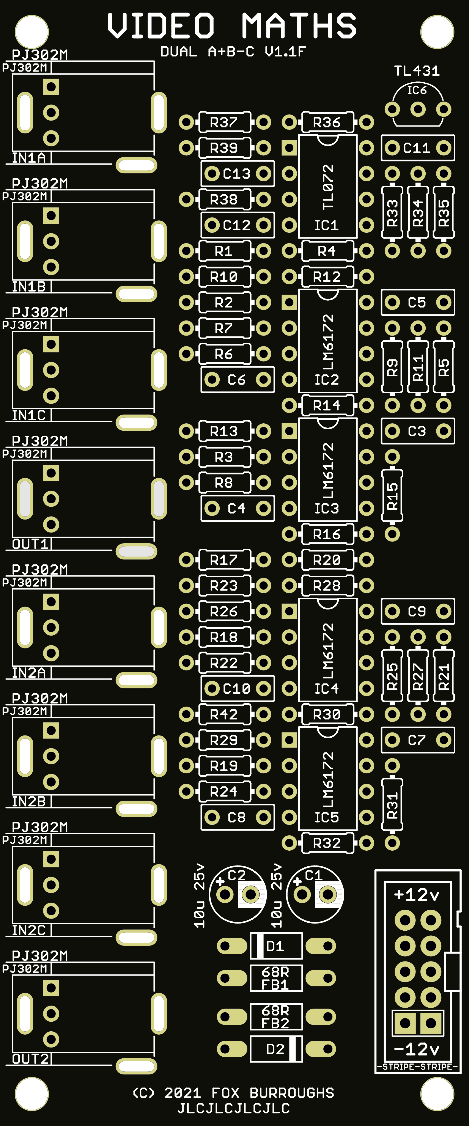
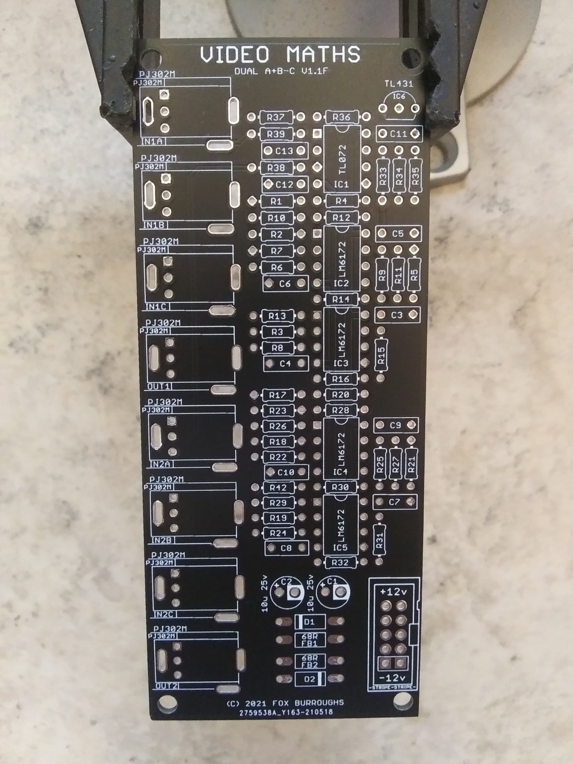
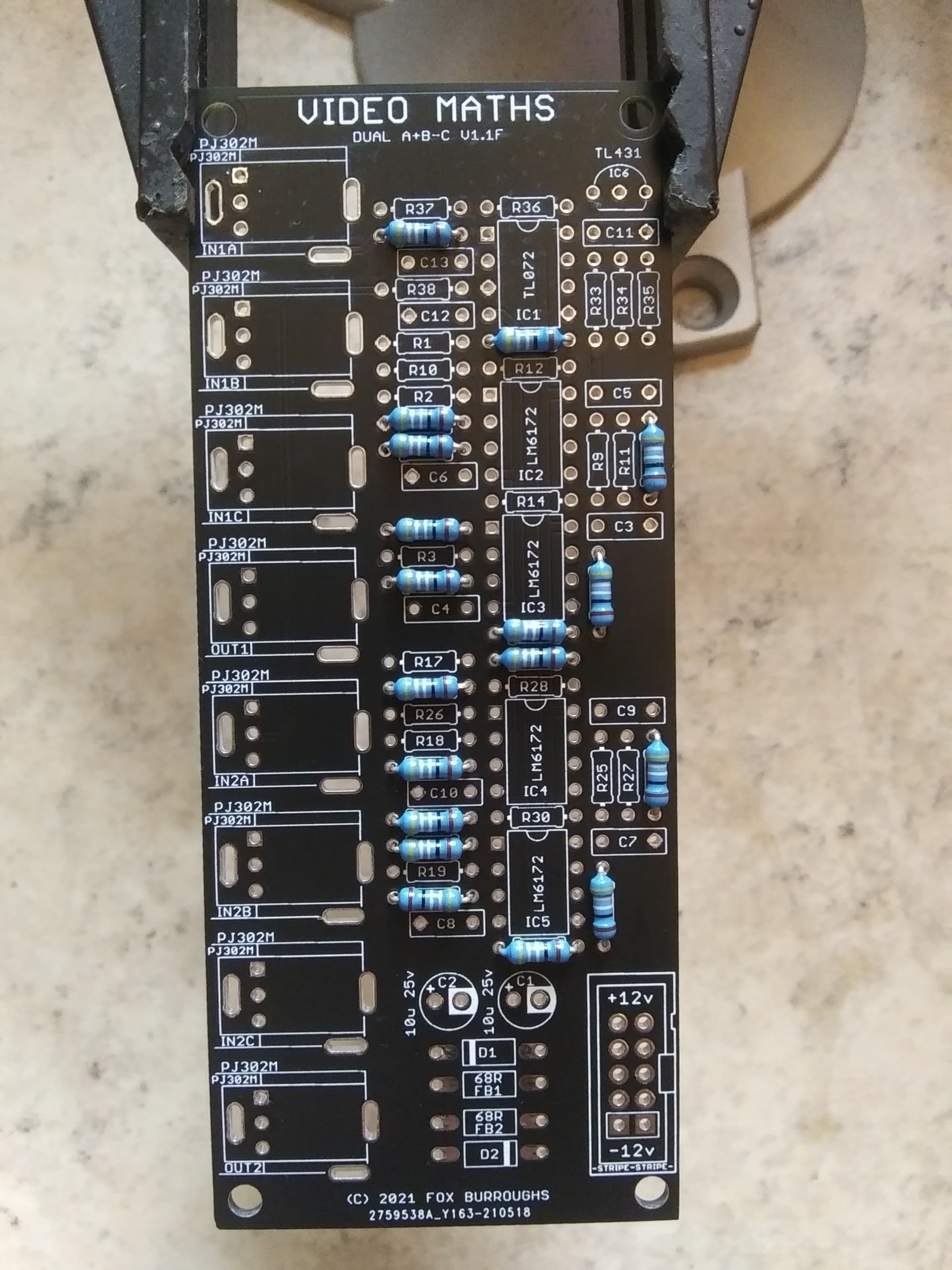
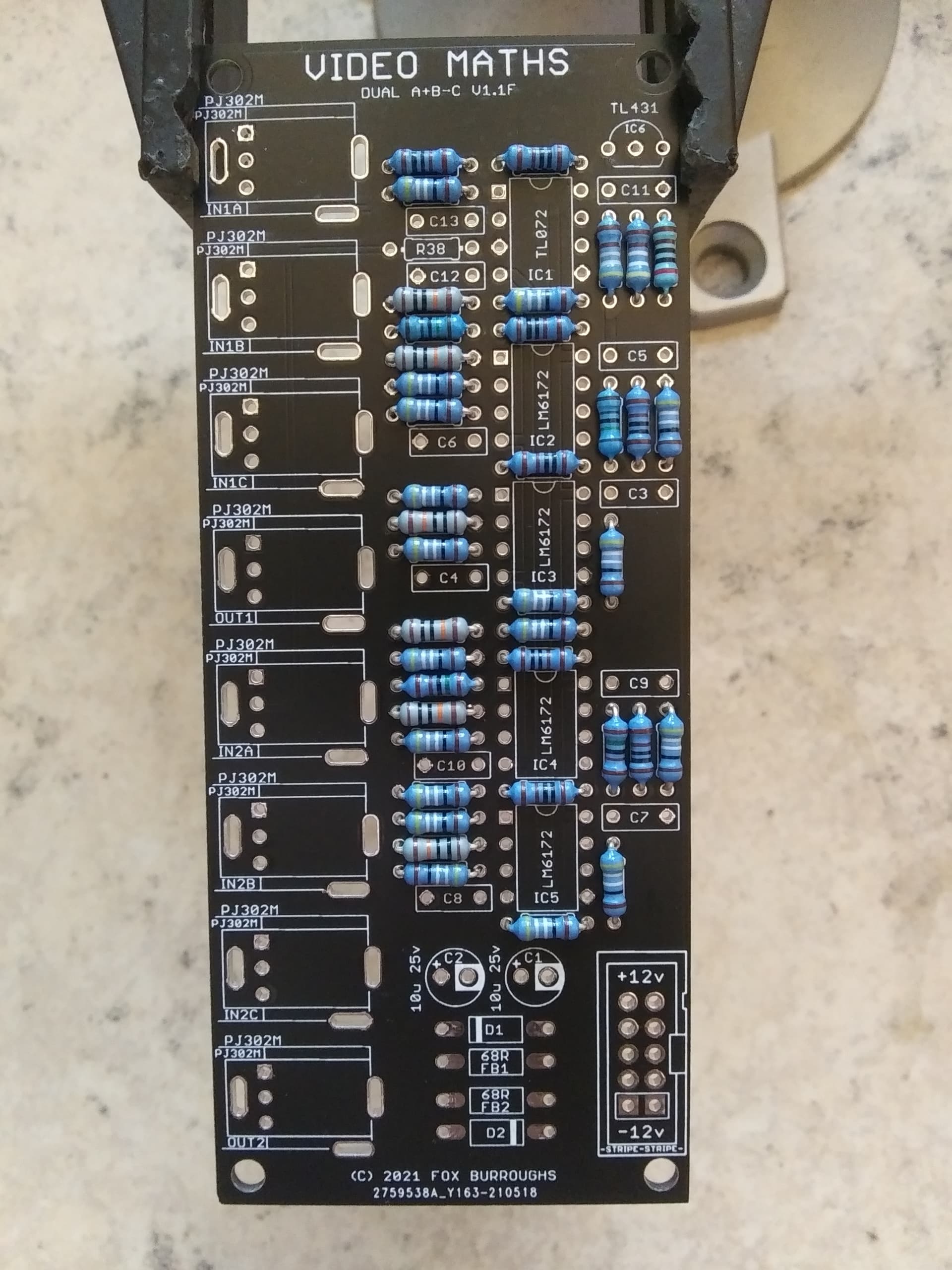
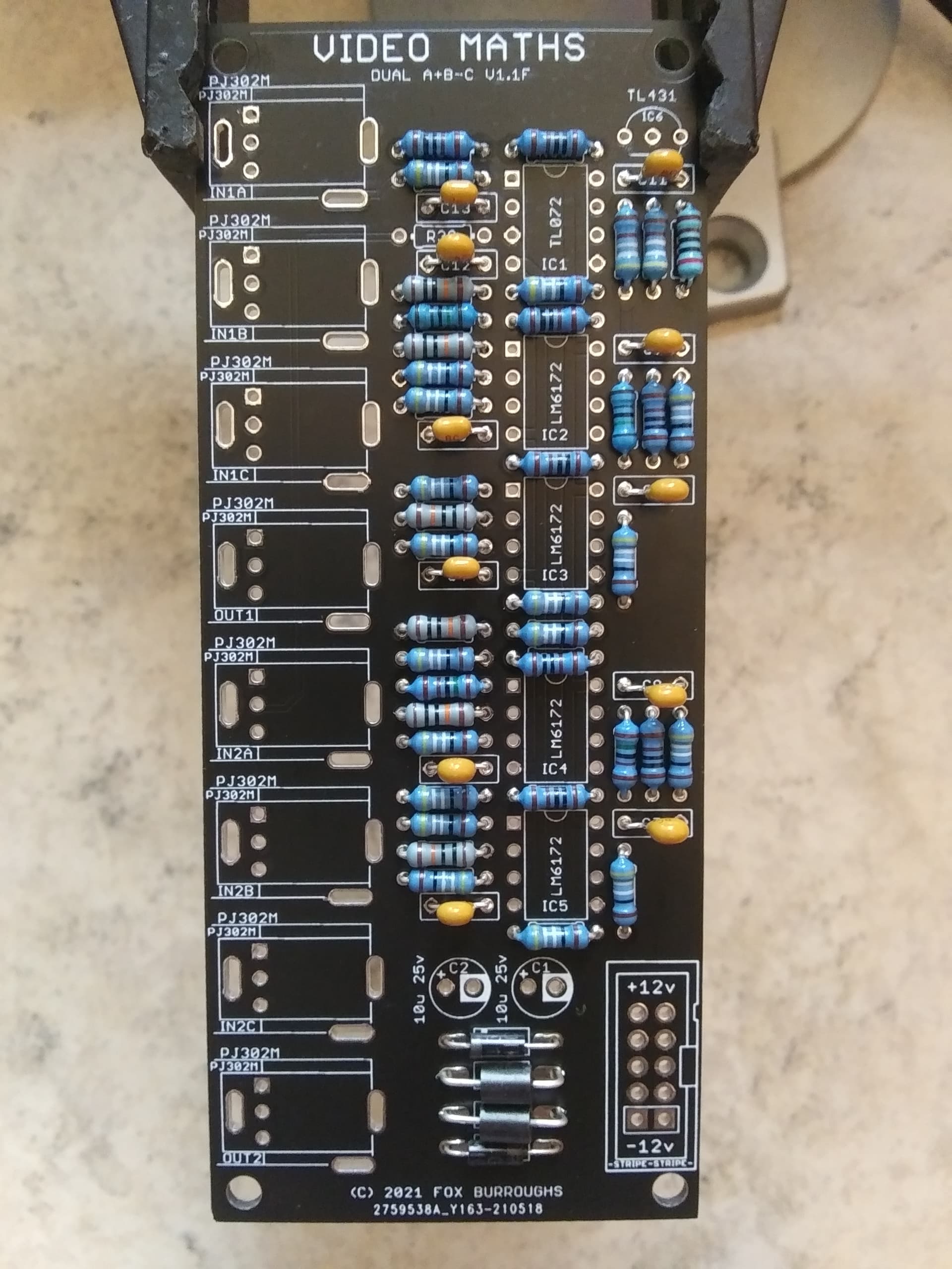
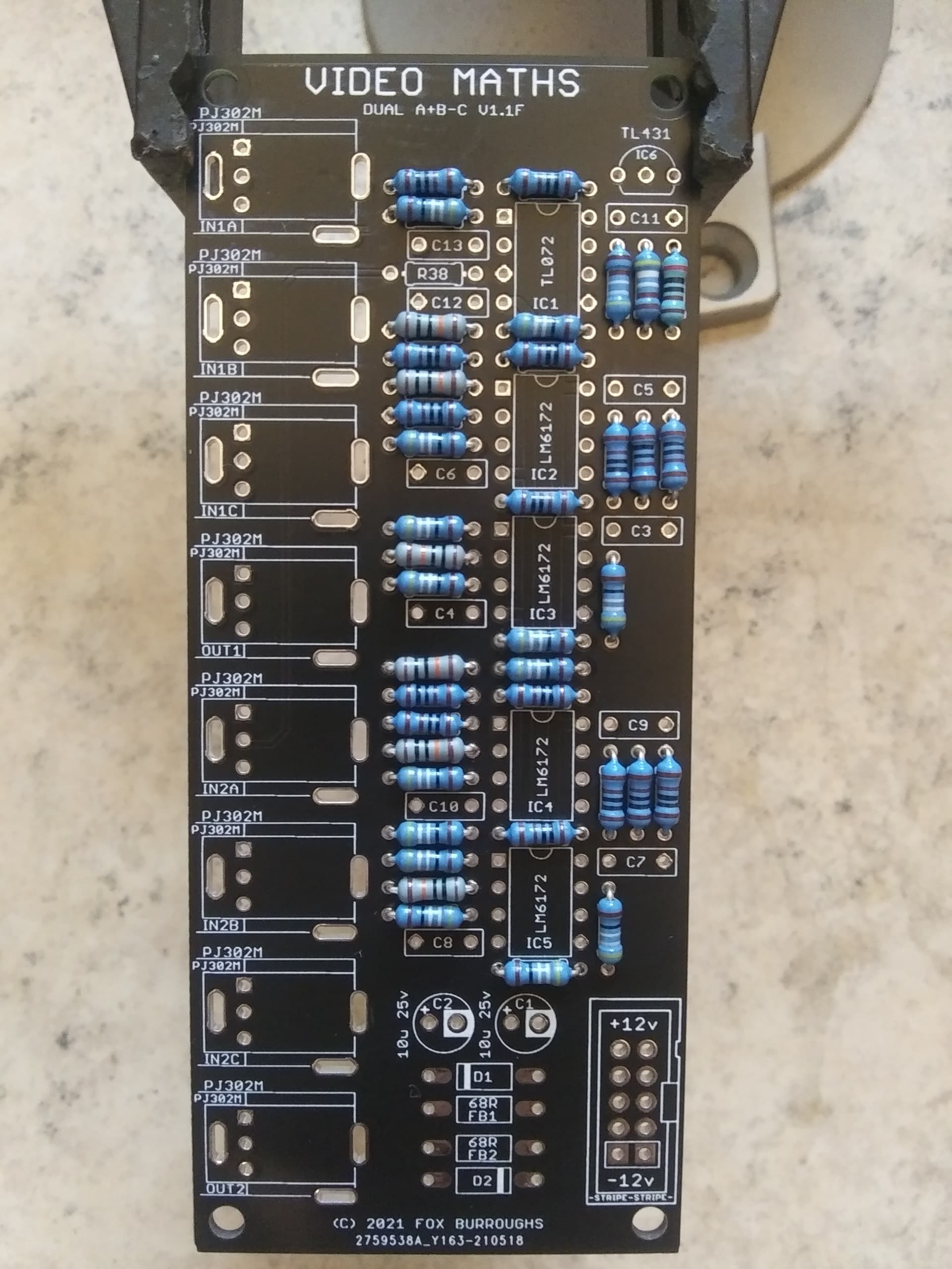
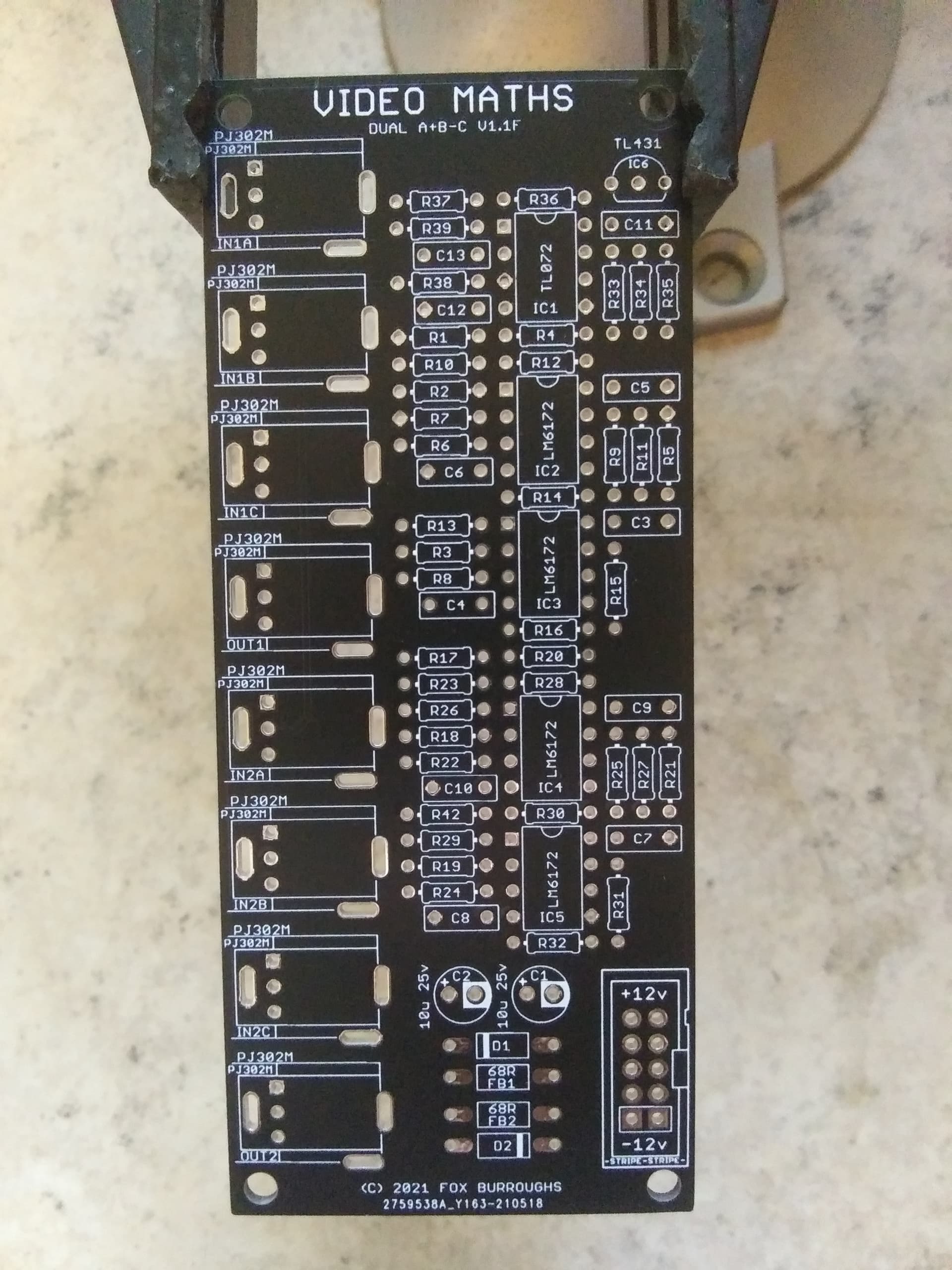
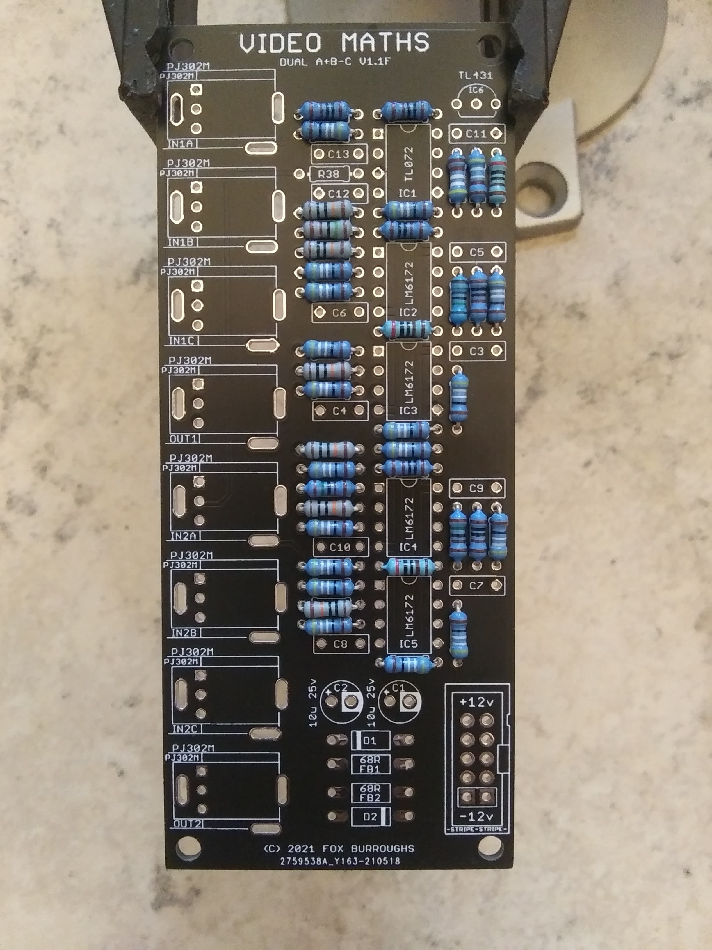
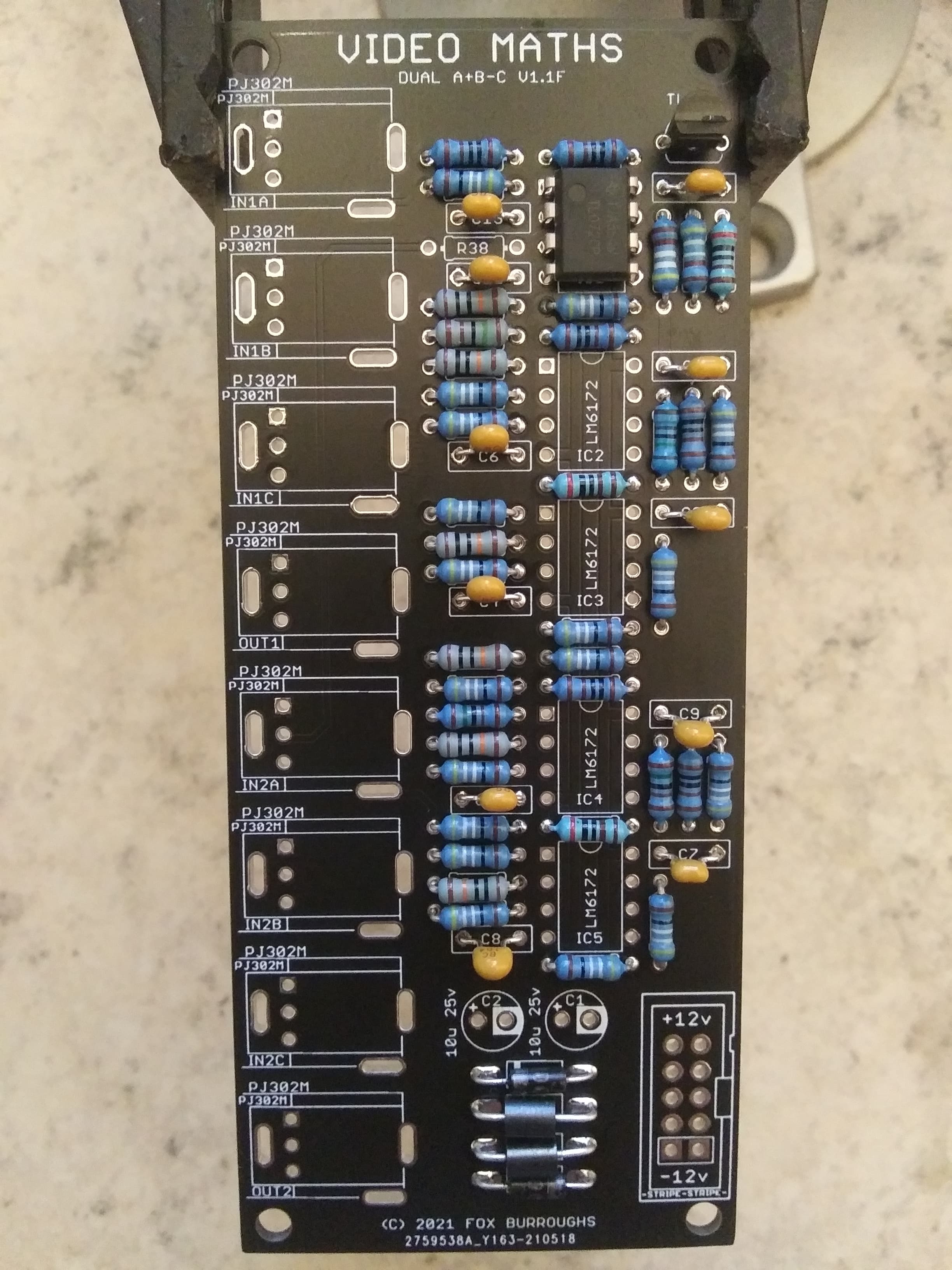
BOM for A+B-C configurationQtyValueParts110-Pin Box Header CONN912K resistorR351TL072 ICIC11TL431 referenceIC6210u/25v capacitorC1, C221N4001 diodeD1, D224.99K resistorR33, R34268R ferrite beadFB1, FB241.5K resistorR9, R10, R25, R264LM6172 ICIC2, IC3, IC4, IC56100K resistorR1, R2, R3, R17, R18, R1981K resistorR11, R12, R14, R27, R28, R30, R36, R378PJ302M jackIN1A, IN1B, IN1C, IN2A, IN2B, IN2C, OUT1, OUT211100n capacitorC3, C4, C5, C6, C7, C8, C9, C10, C11, C12, C1318499R resistorR4, R5, R6, R7, R8, R13, R15, R16, R20, R21, R22, R23, R24, R29, R31, R32, R39, R422Solder JumpersJP2, JP41PCB set-110-16 Power ribbon----5DNPR38, JP1, JP3, JP5, JP6*Solder jumpers are located on bottom-side of board.
*DNP means Do not populate.
*Unless specified differently, All resistors are always Metal Film type, 1/4W, 1% tolerance.
Build Guide for A+B-CStep 0.
Using a PCB vice will improve your DIY experience immensely.
Step 1.
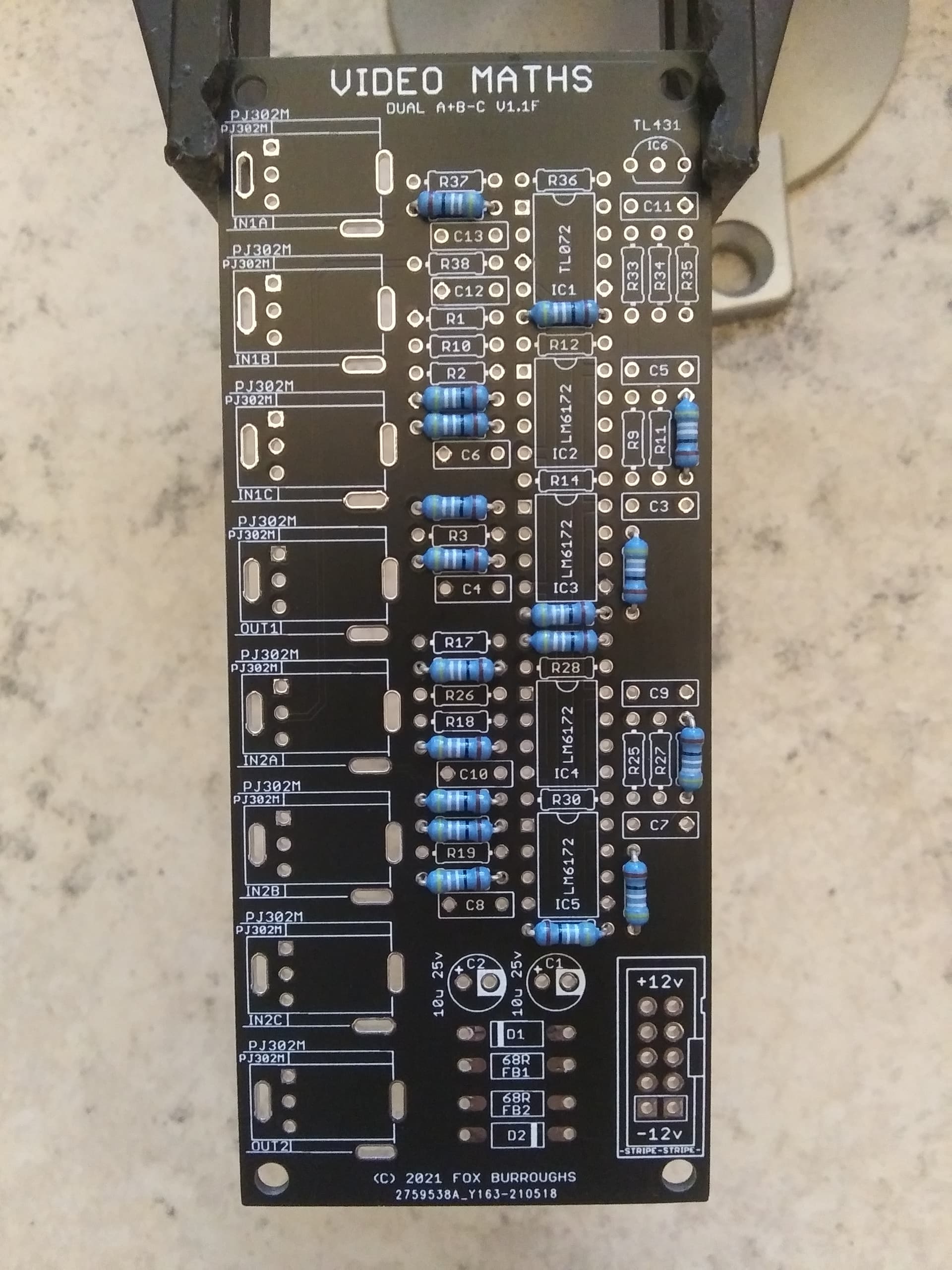
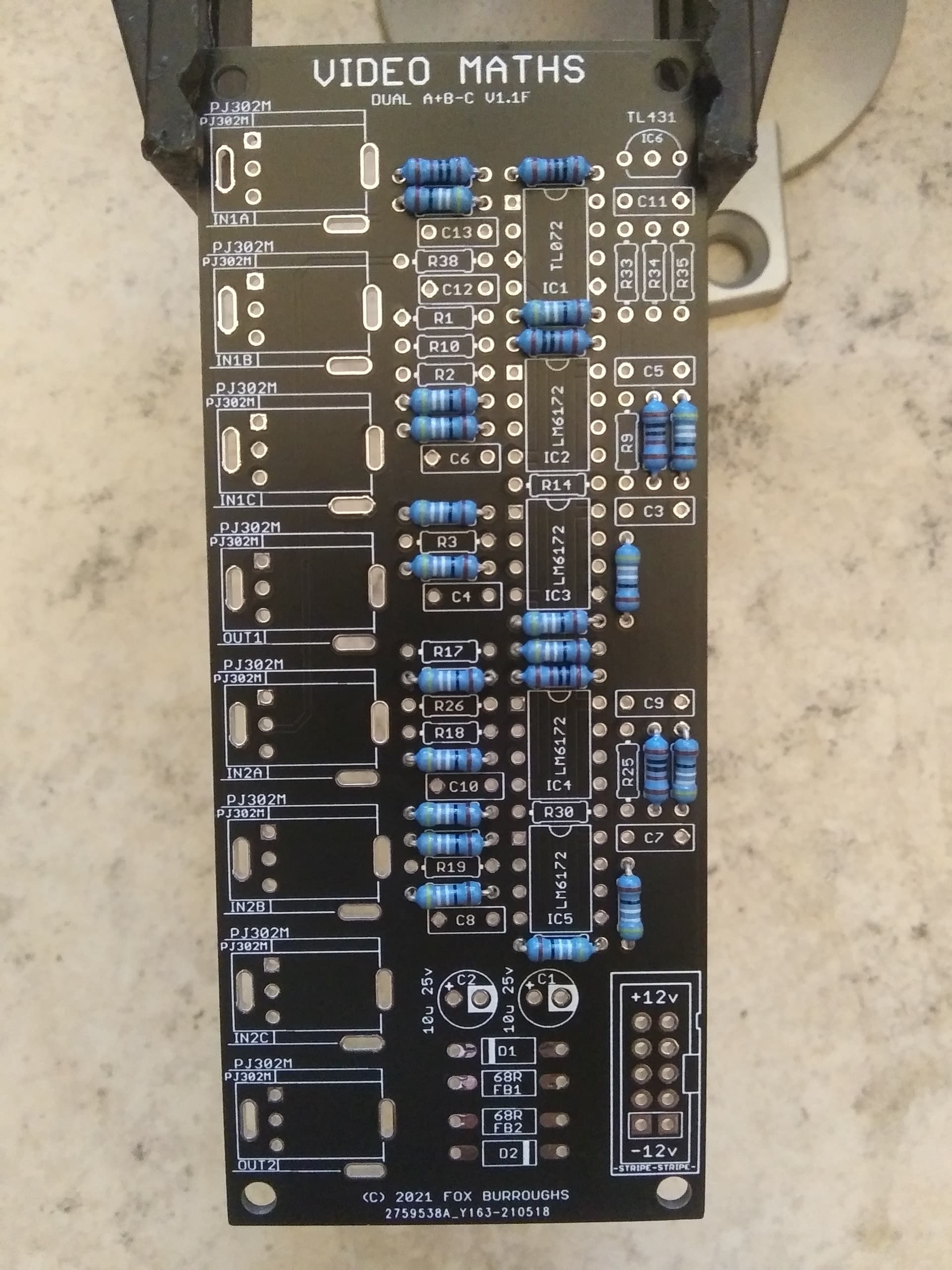
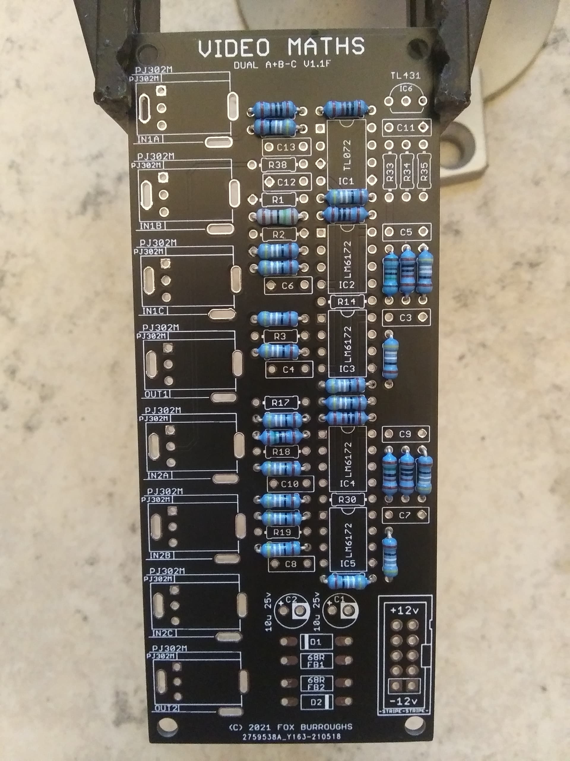
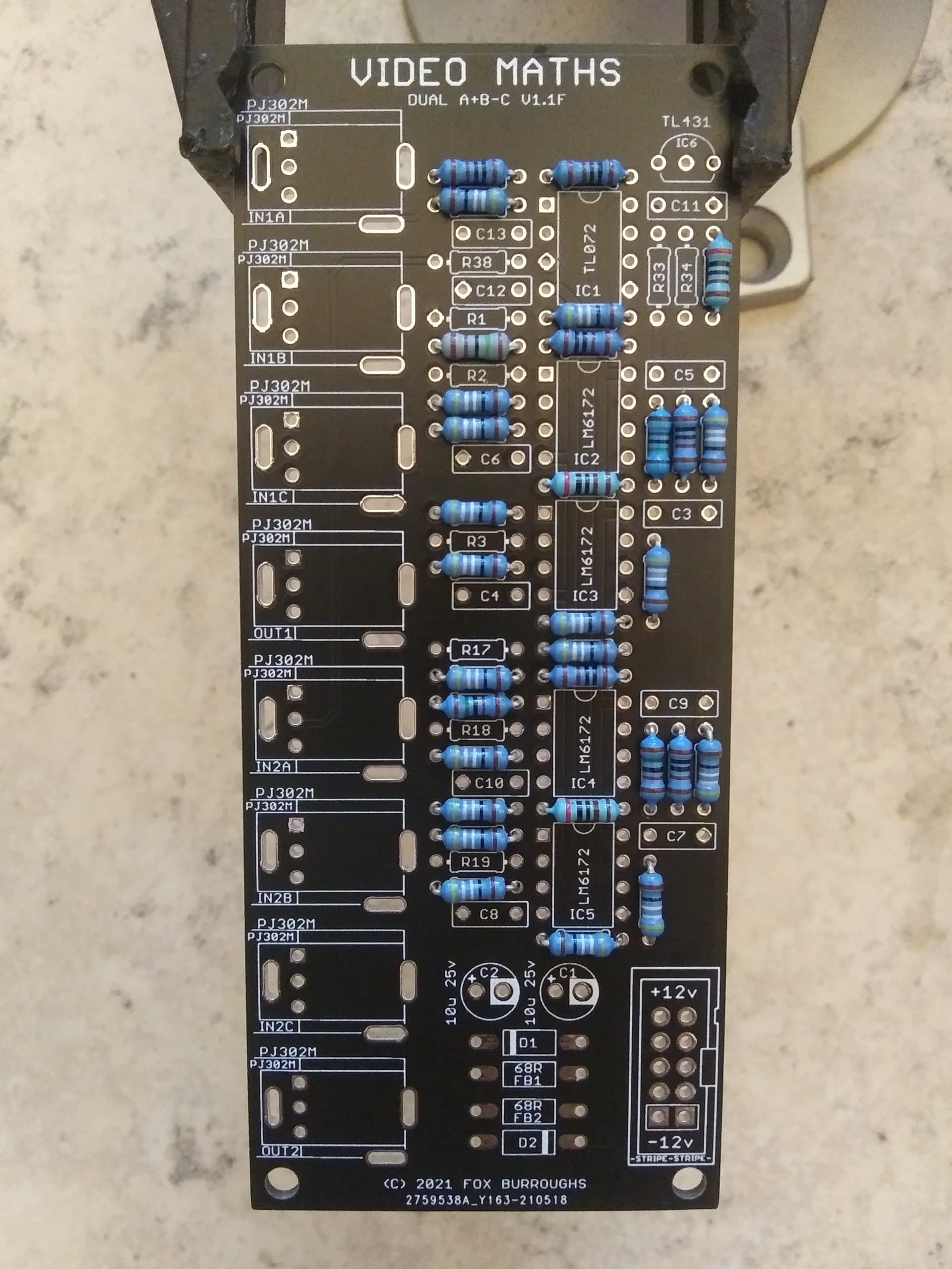
We will being with the 499R resistors. There are 18 of them: R4, R5, R6, R7, R8, R13, R15, R16, R20, R21, R22, R23, R24, R29, R31, R32, R39, R42.
Step 2.
Next are the 1K resistors: R11, R12, R14, R27, R28, R30, R36, R37
Step 3.
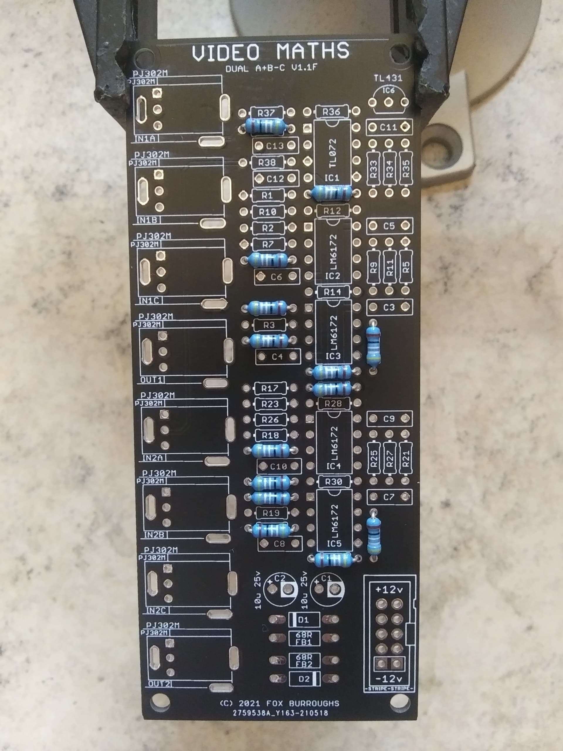
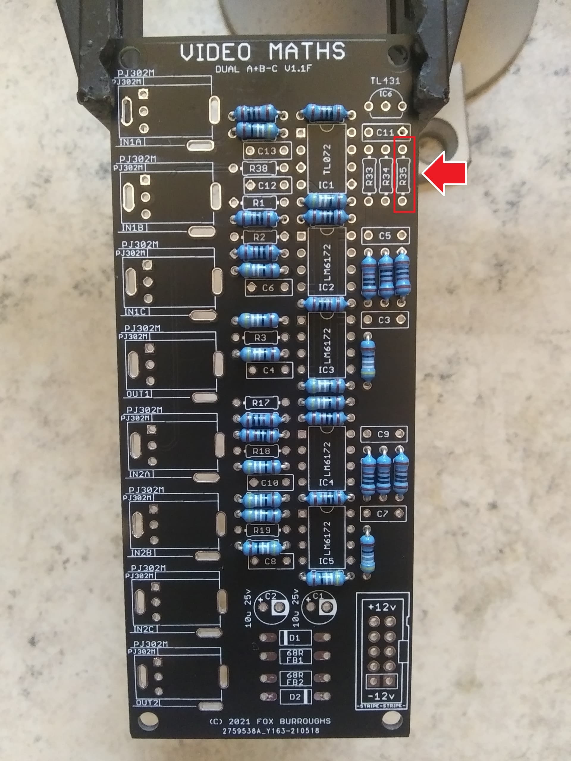
Just a single 2K resistor for this config, R35.
Step 4.
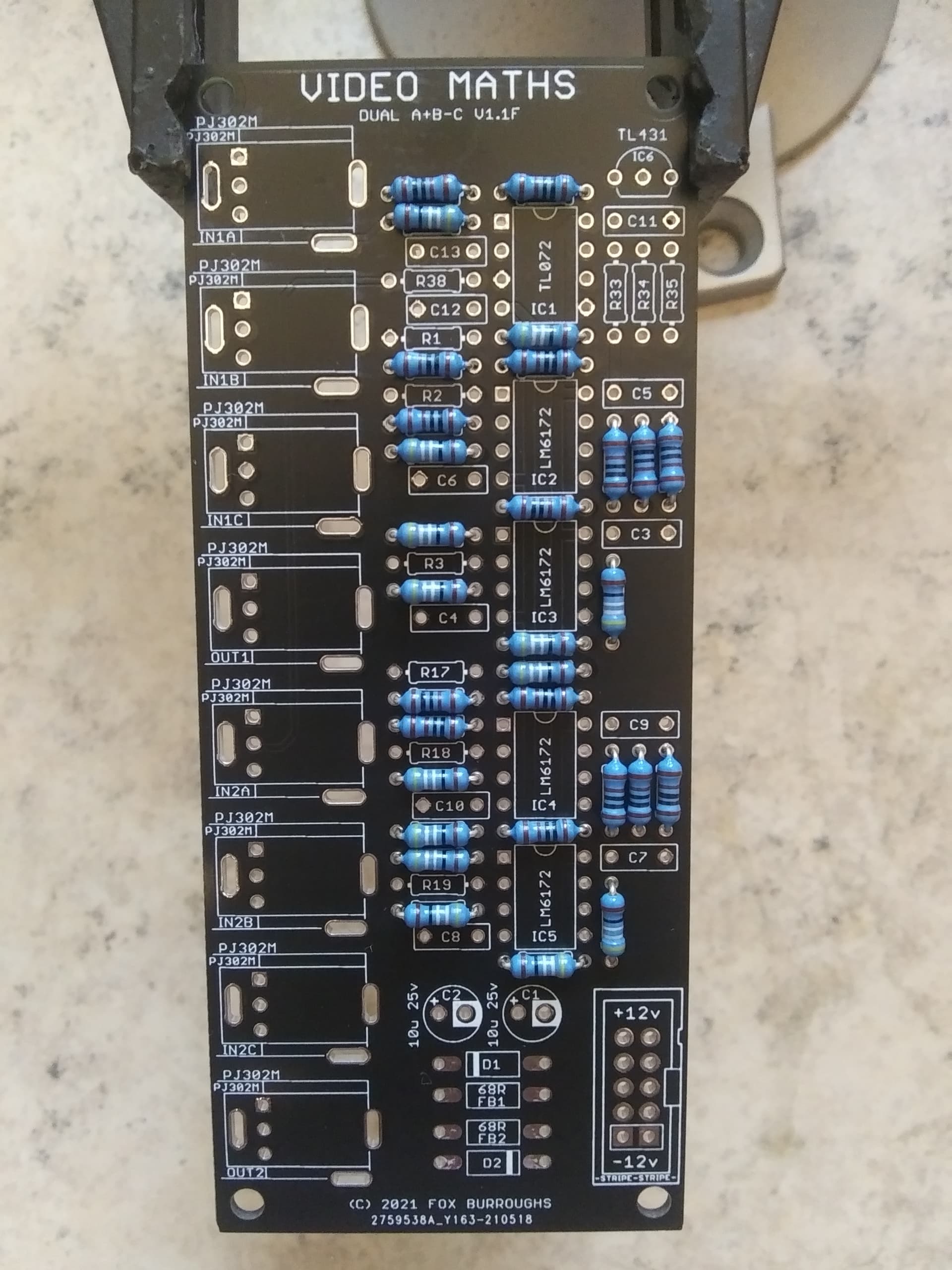
Next are two 4.99K resistors: R33, R34.
Step 5.
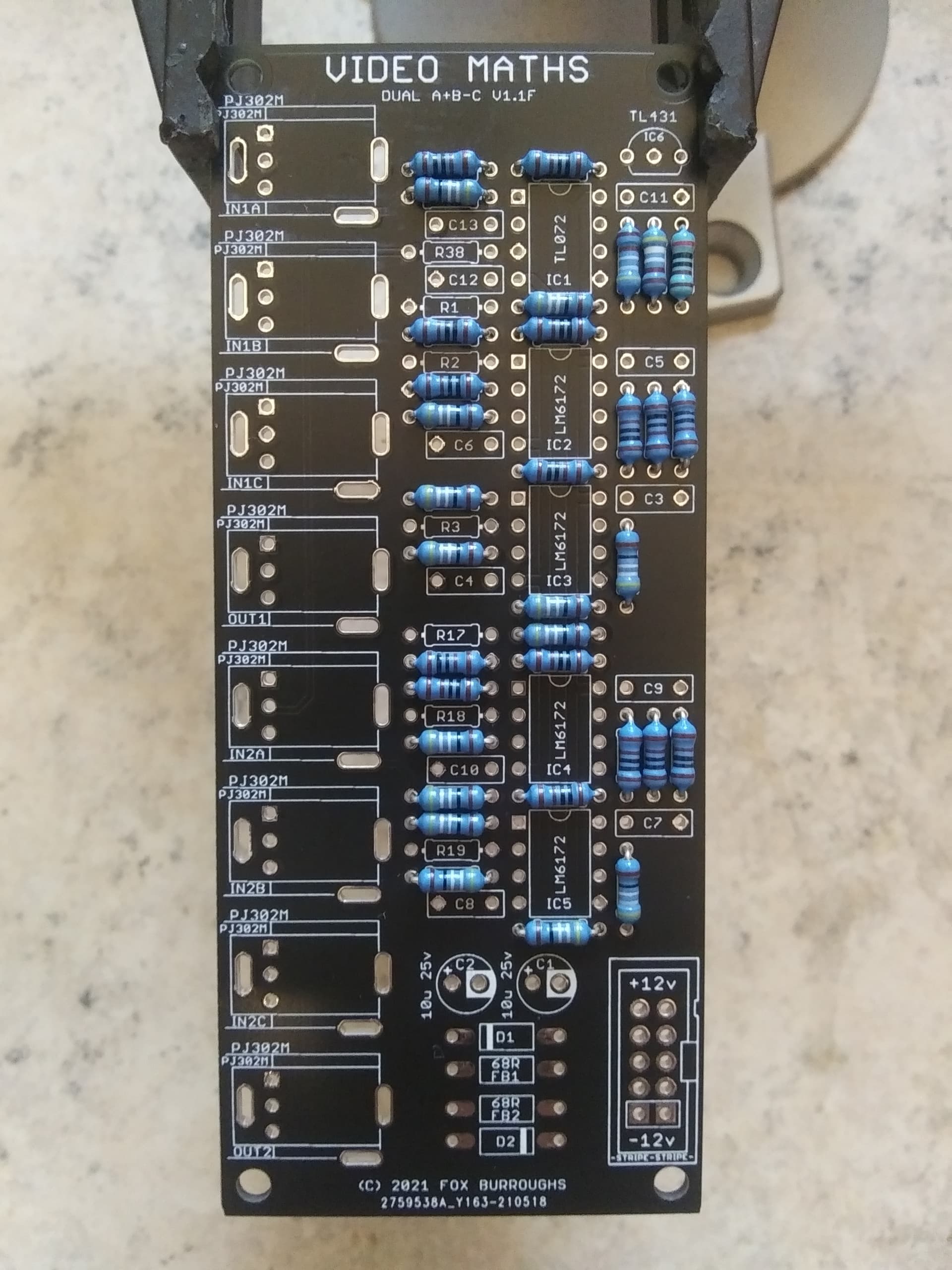
Six 100K resistors, R1, R2, R3, R17, R18, R19.
Step 6.
The last four resistors are 1.5K ohms: R9, R10, R25, R26.
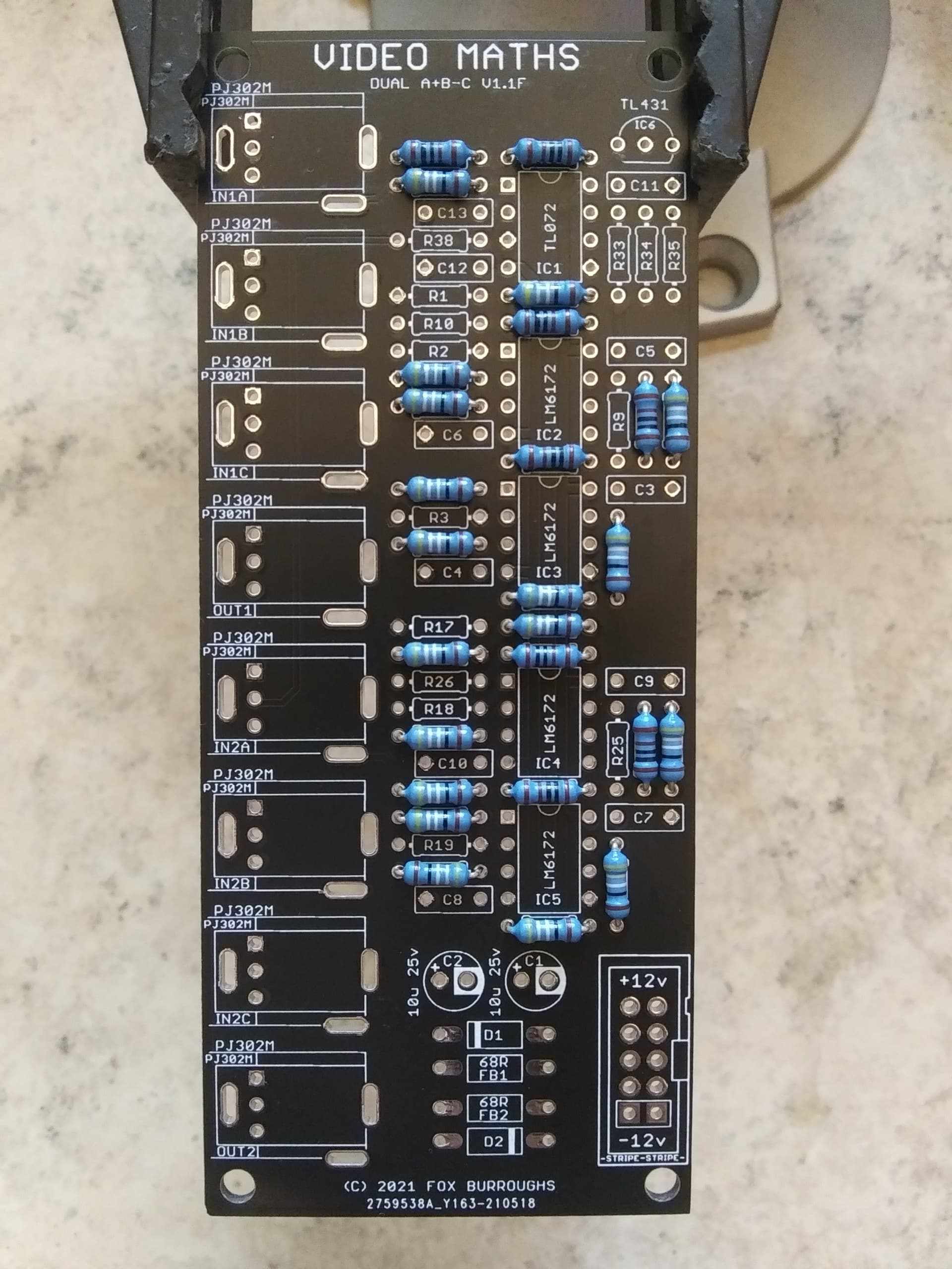
Step 7.
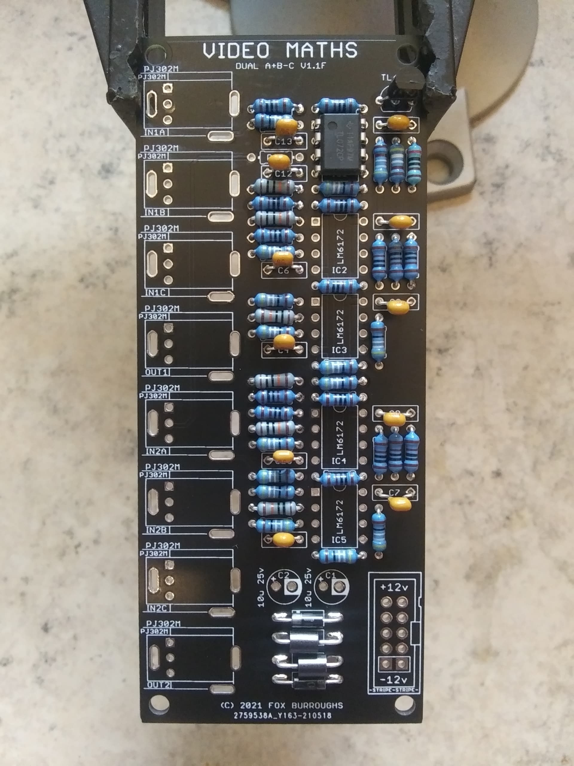
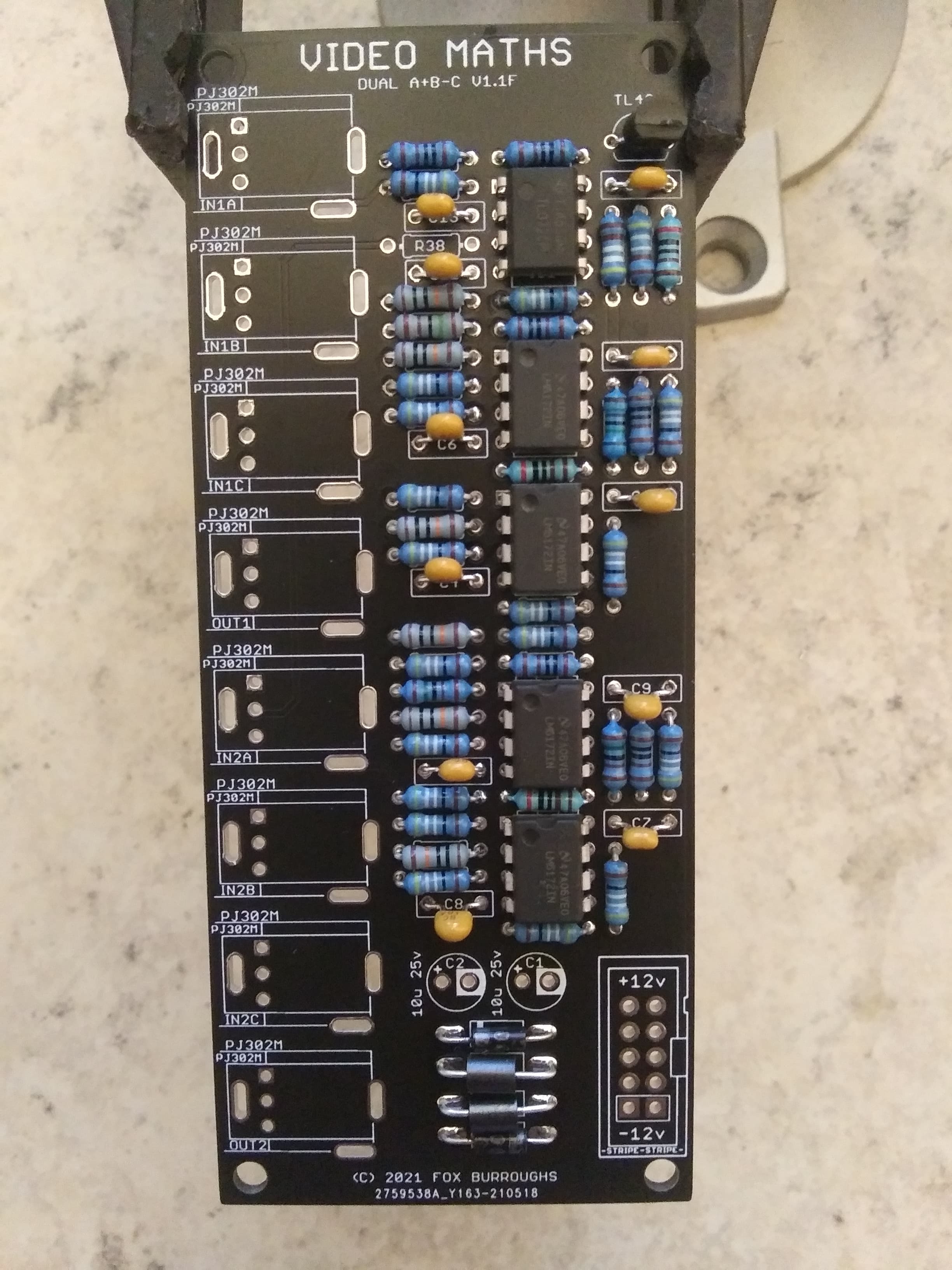
Here you can see that I’ve populated all eleven 100nF caps as well as both diodes and both ferrite beads. As always, make sure the stripes on the diodes line up with the stripes on the pcb.
Step 8.
Next, add the TL431 voltage reference to the top right hand side of the pcb.
Step 9.
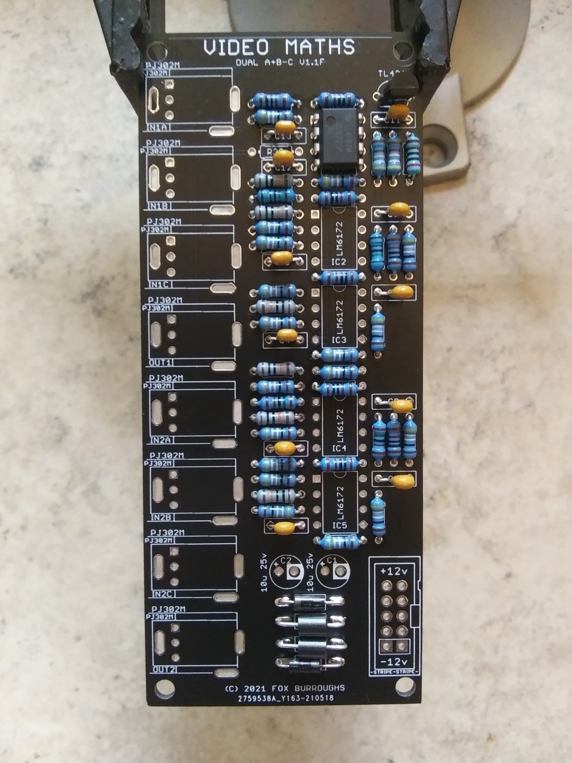
The top op amp is a TL072. Make sure pin 1 is lined up with the square via.
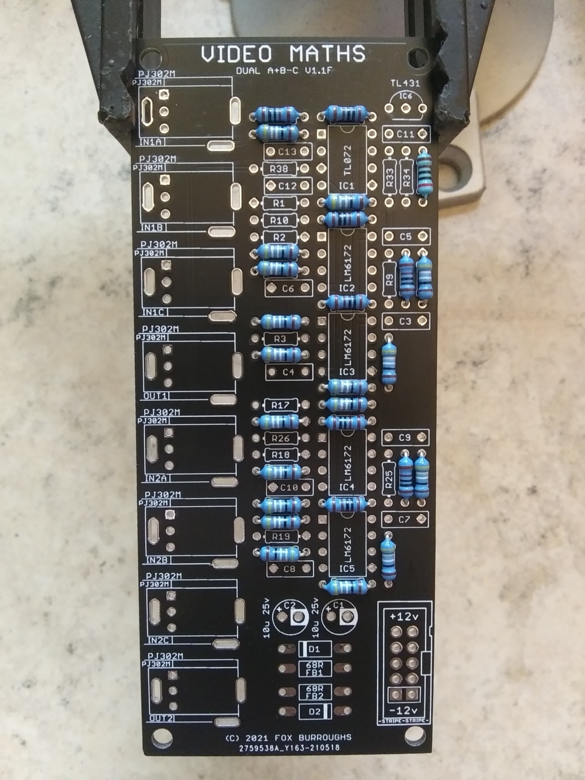
Step 10.
The four remaining op amps are LM6172’s. Again, make sure pin 1 of each IC is lined up with the square vias.
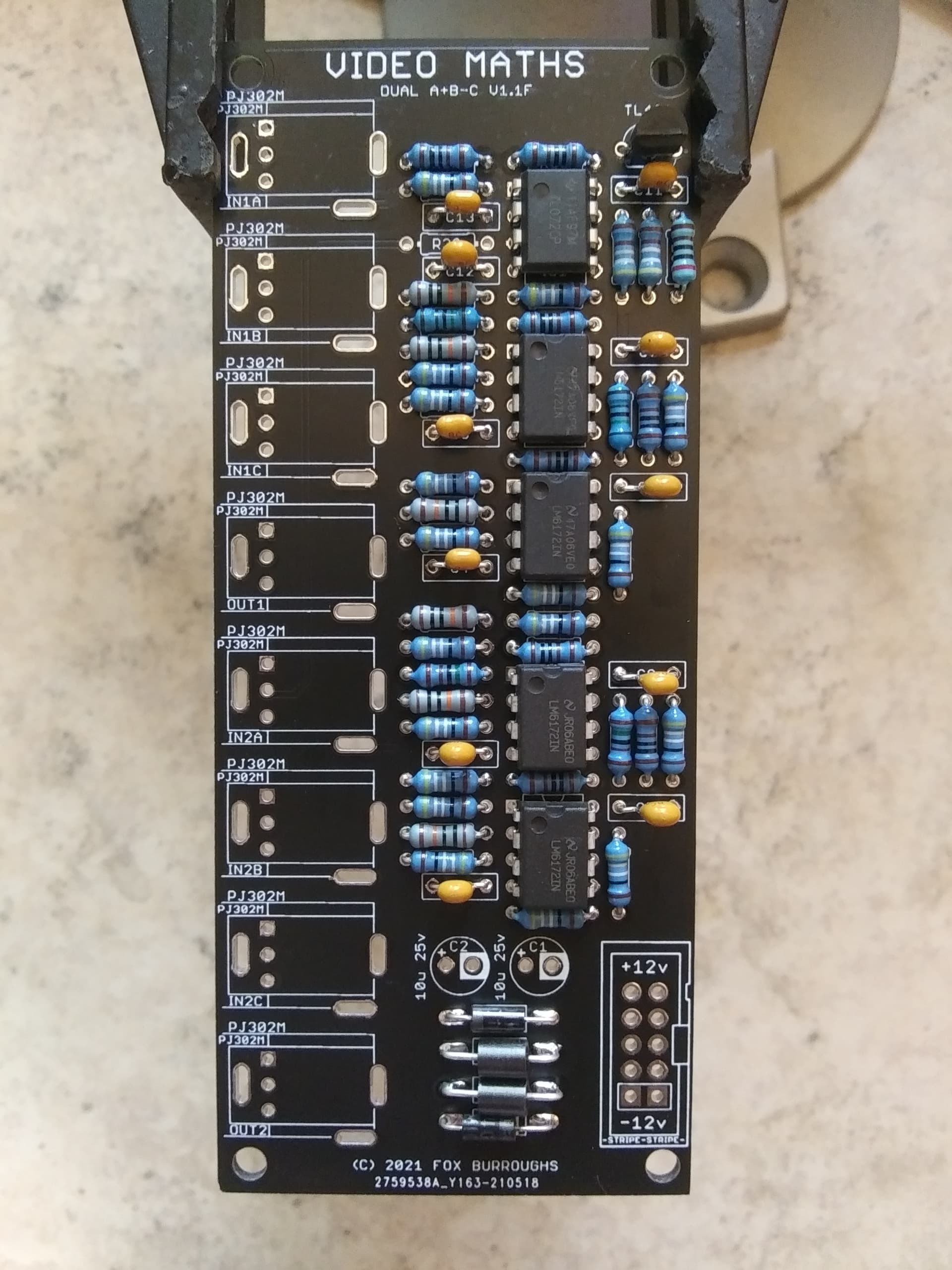
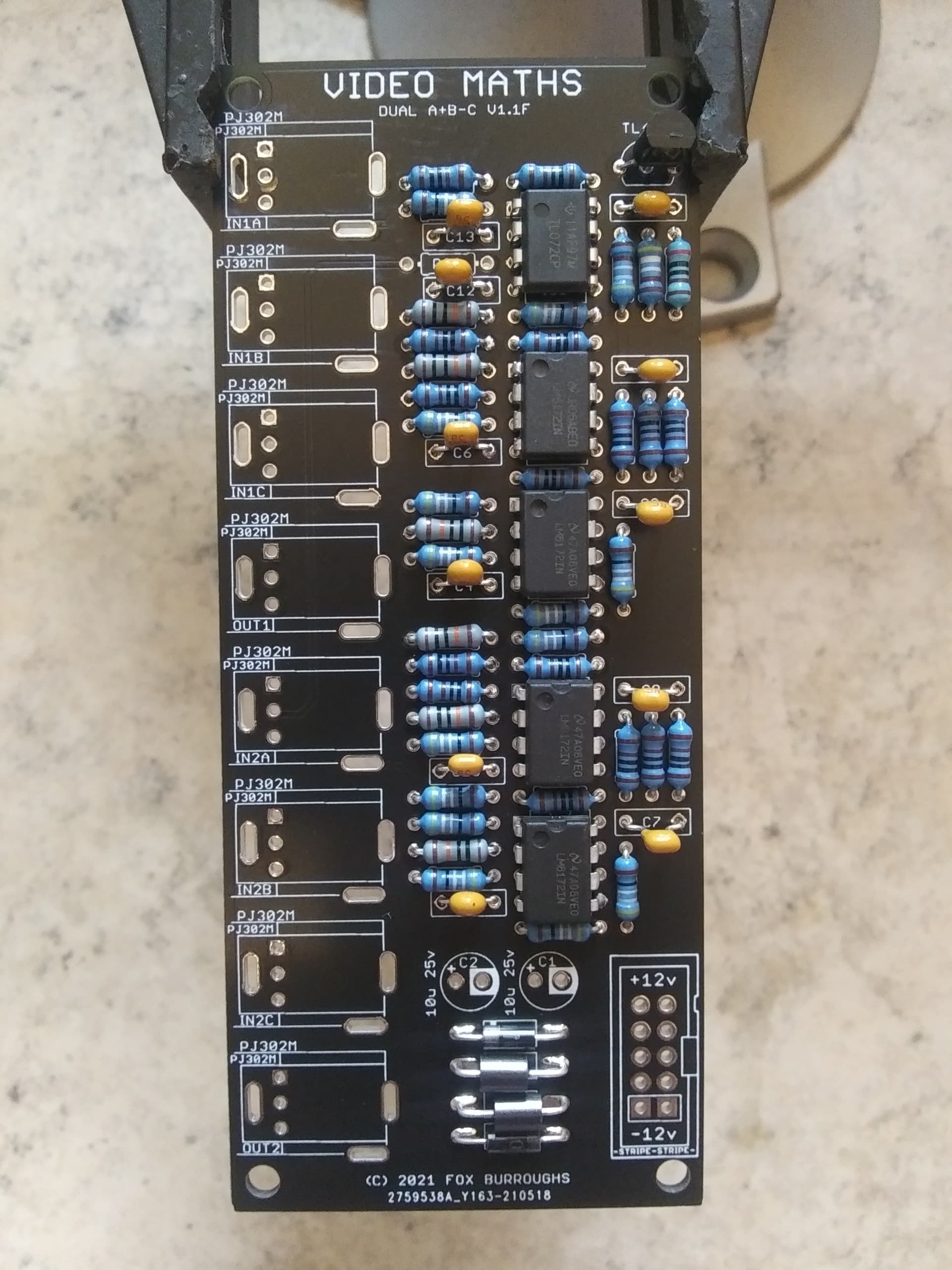
Step 11.
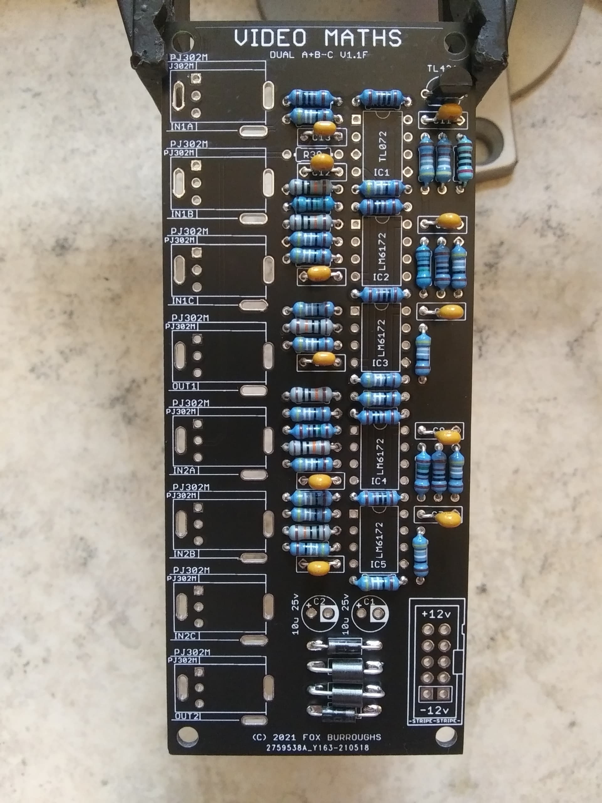
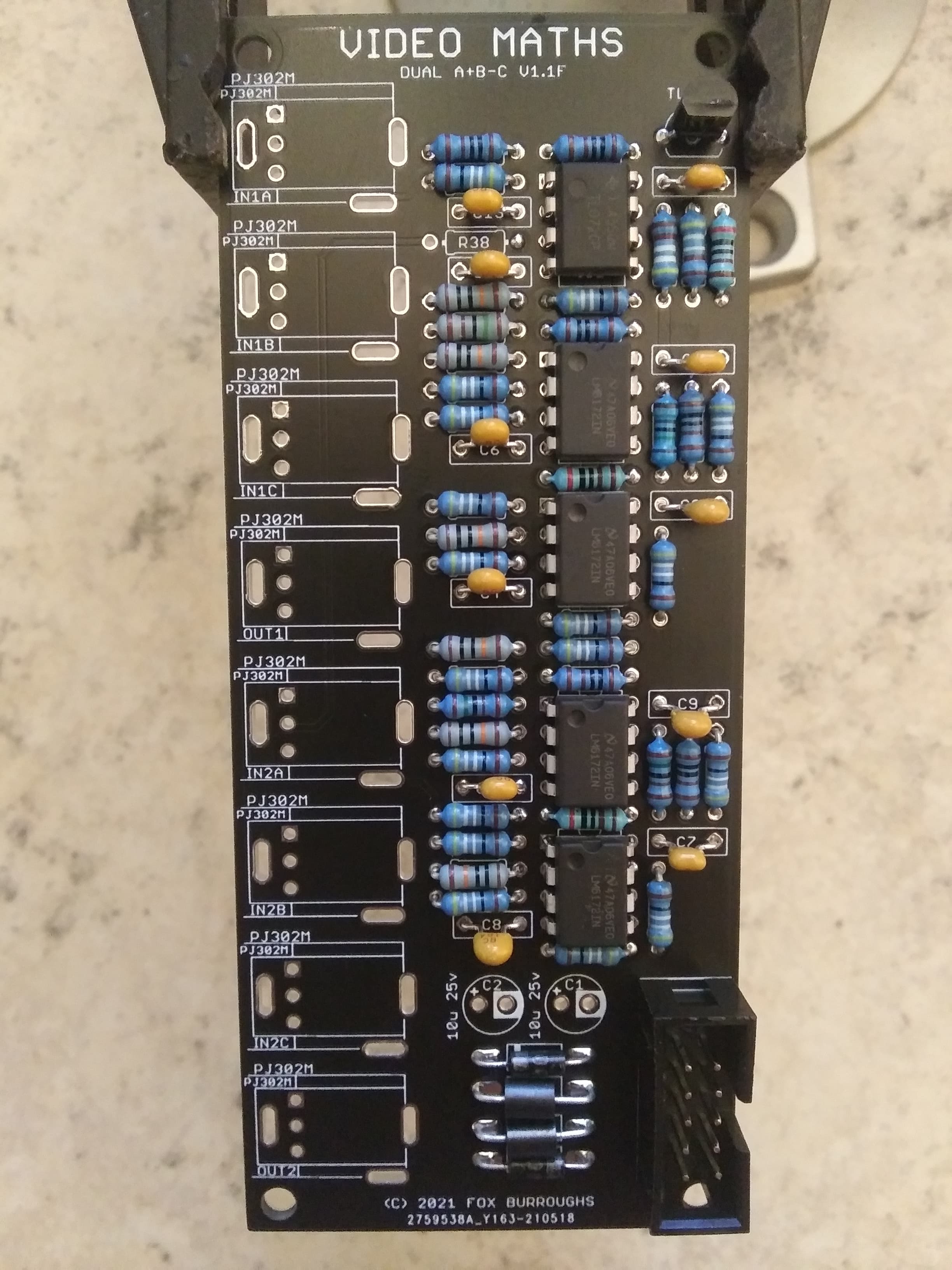
The next tallest component is the 10-pin shrouded power connector. The “notch” or “key” faces outward to the right.
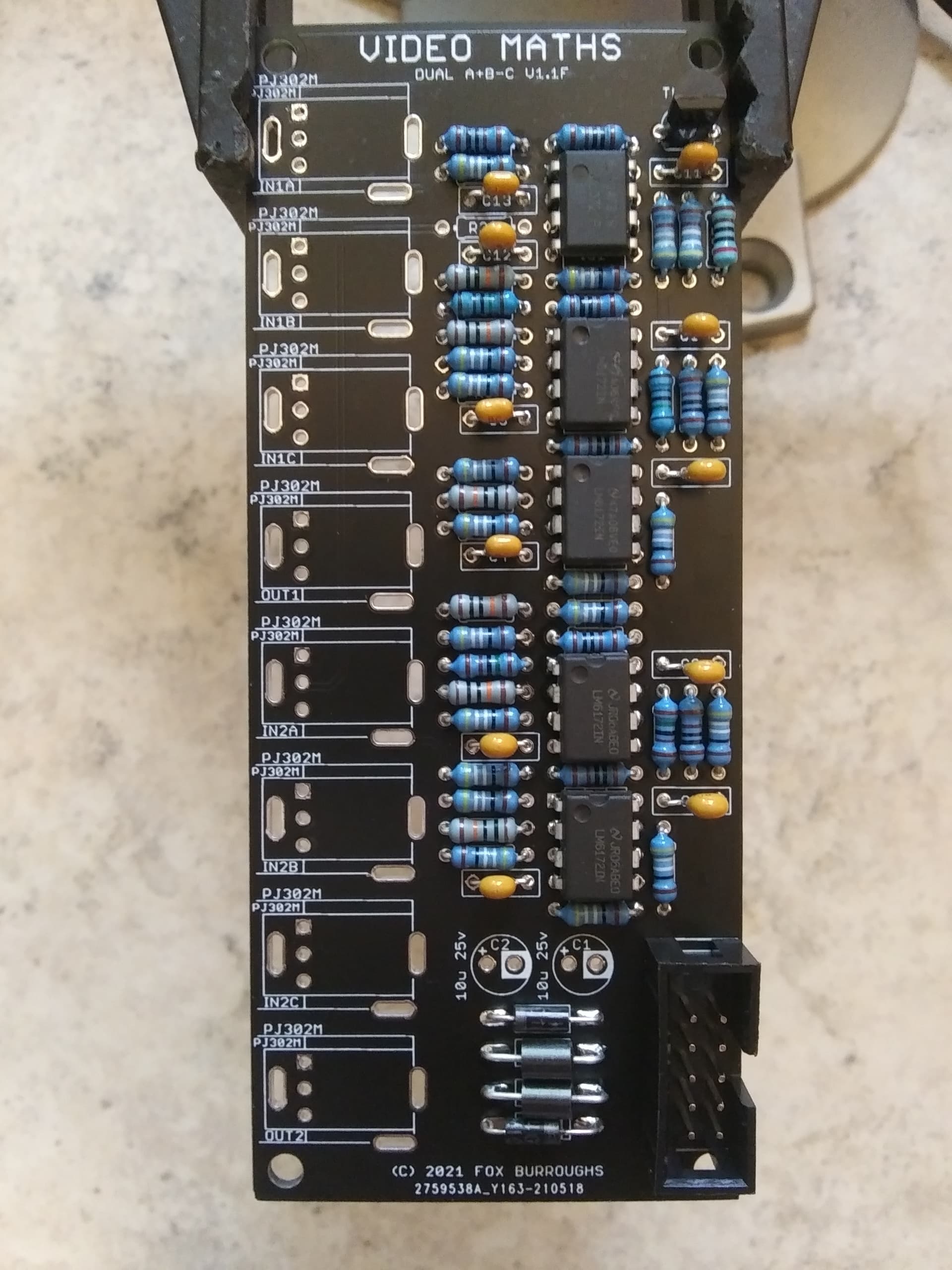
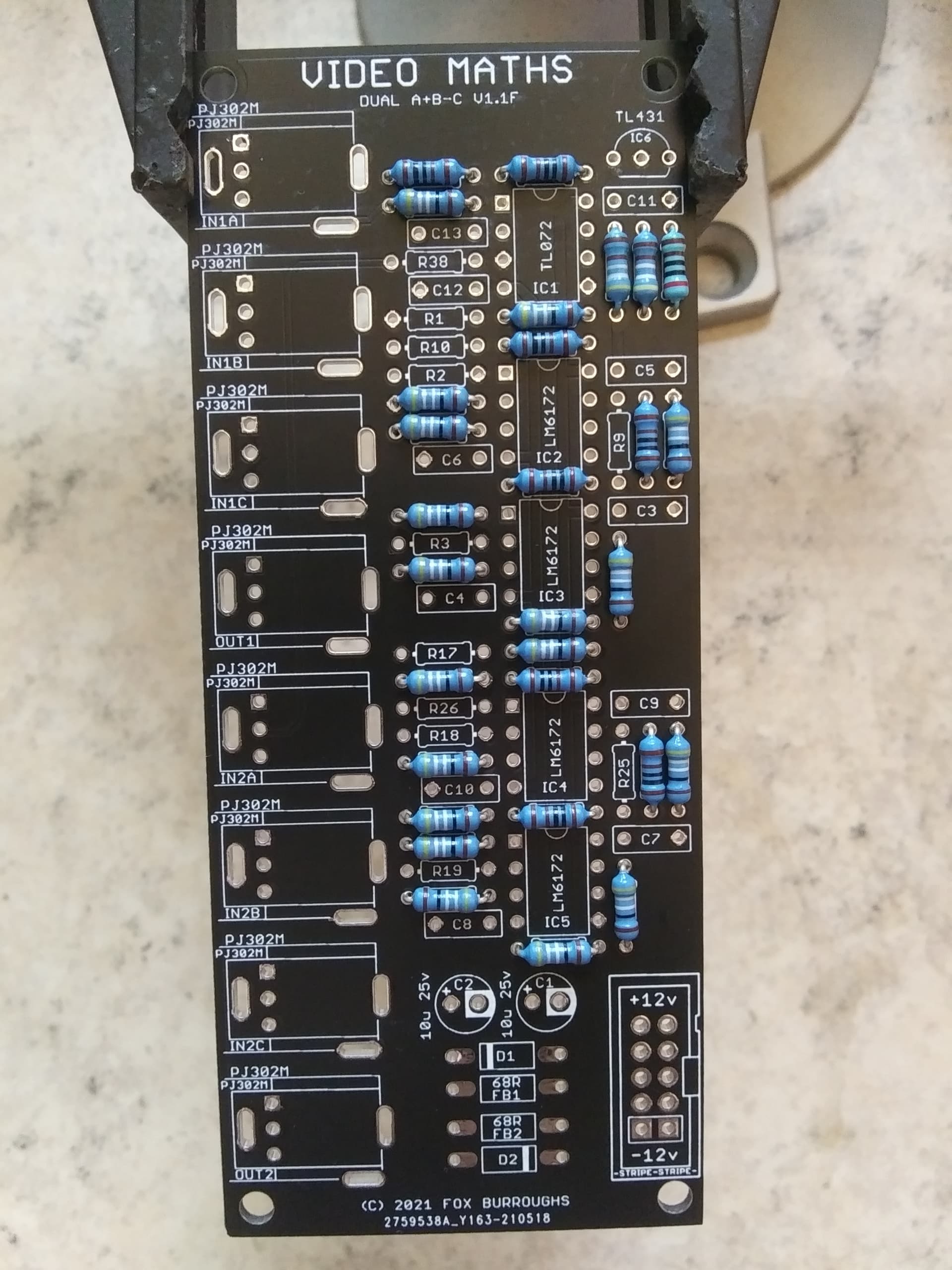
Step 12.
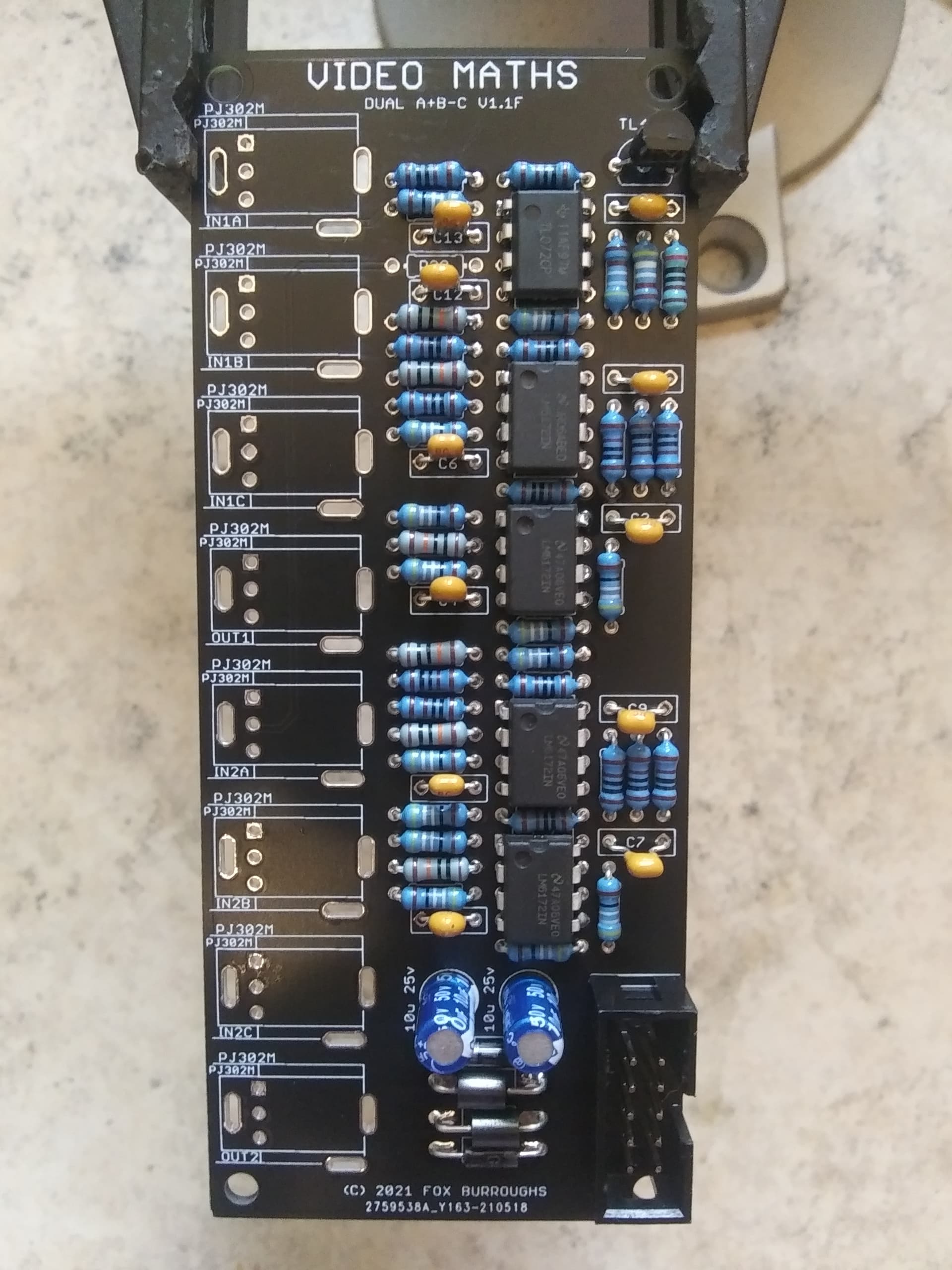
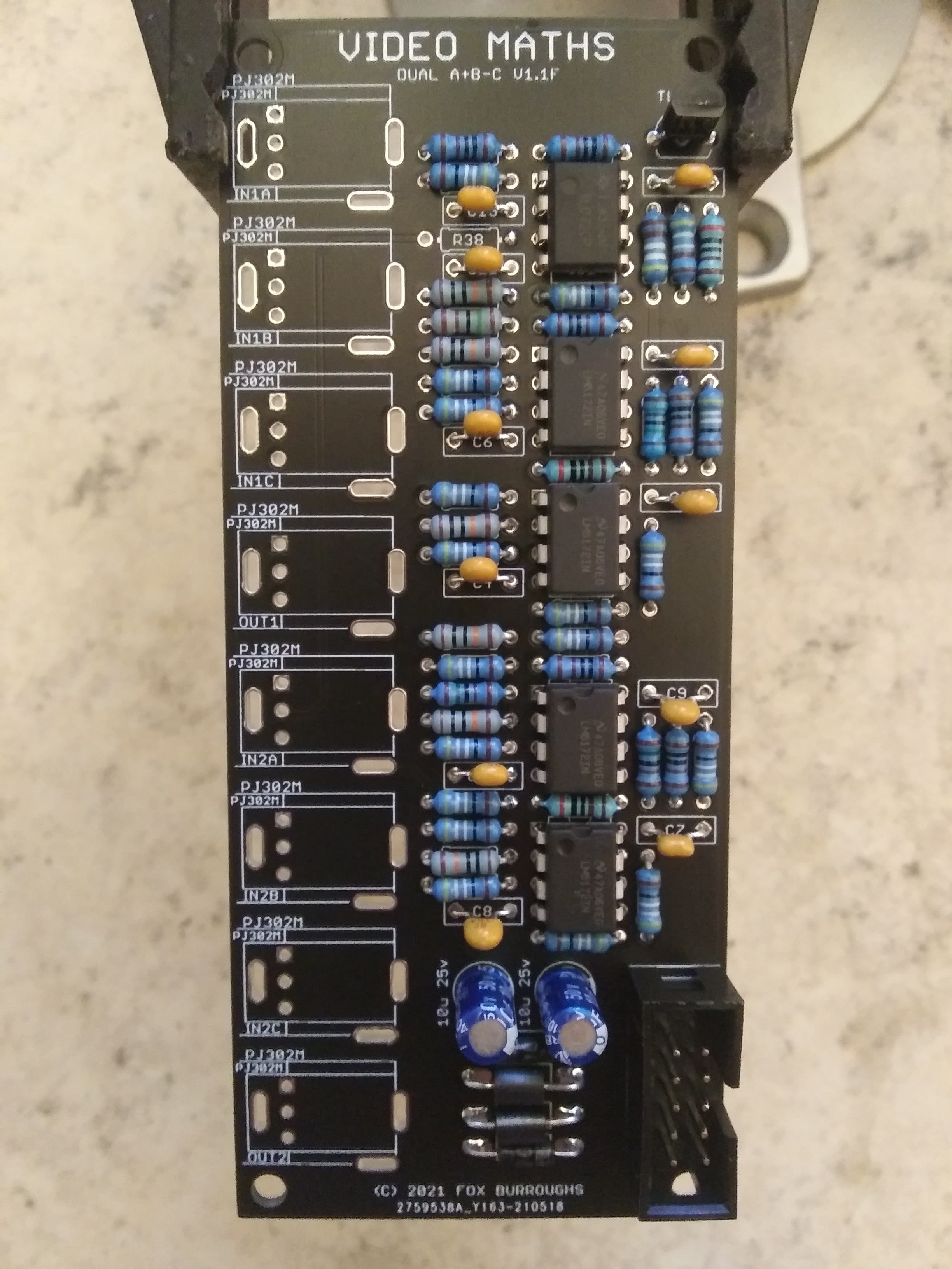
Now populate both electrolytic caps. These are polarized parts and the stripe down the side designates the negative lead. Place the negative lead into the via that is circled.
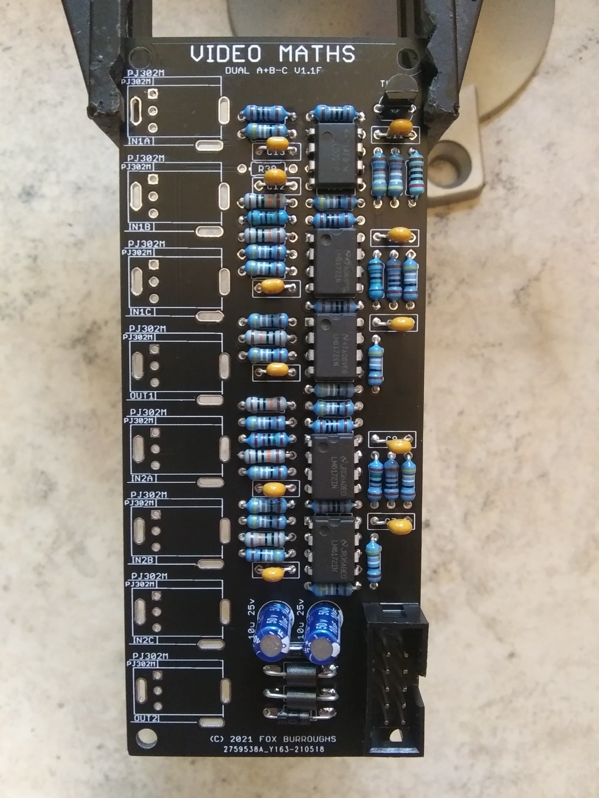
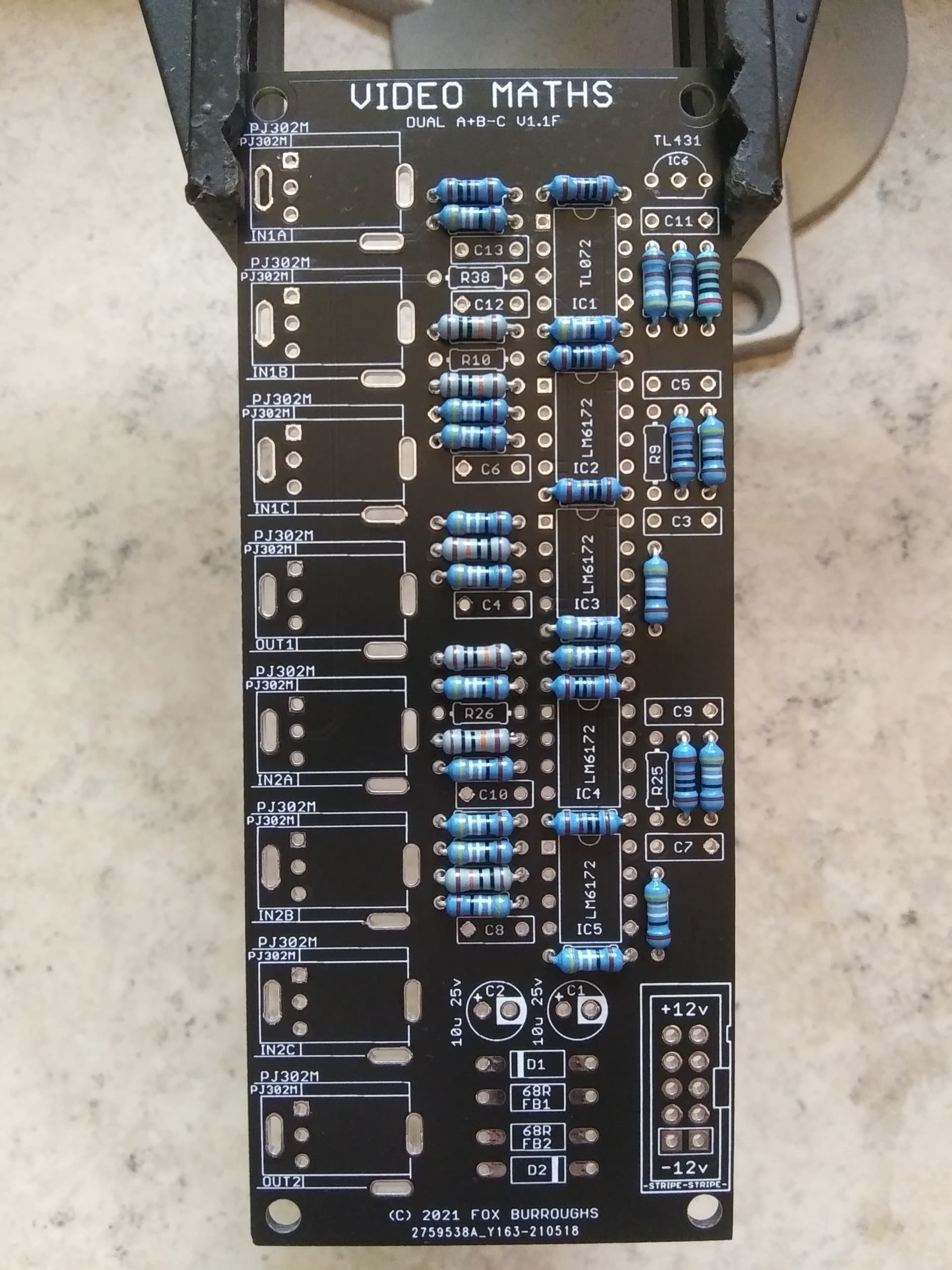
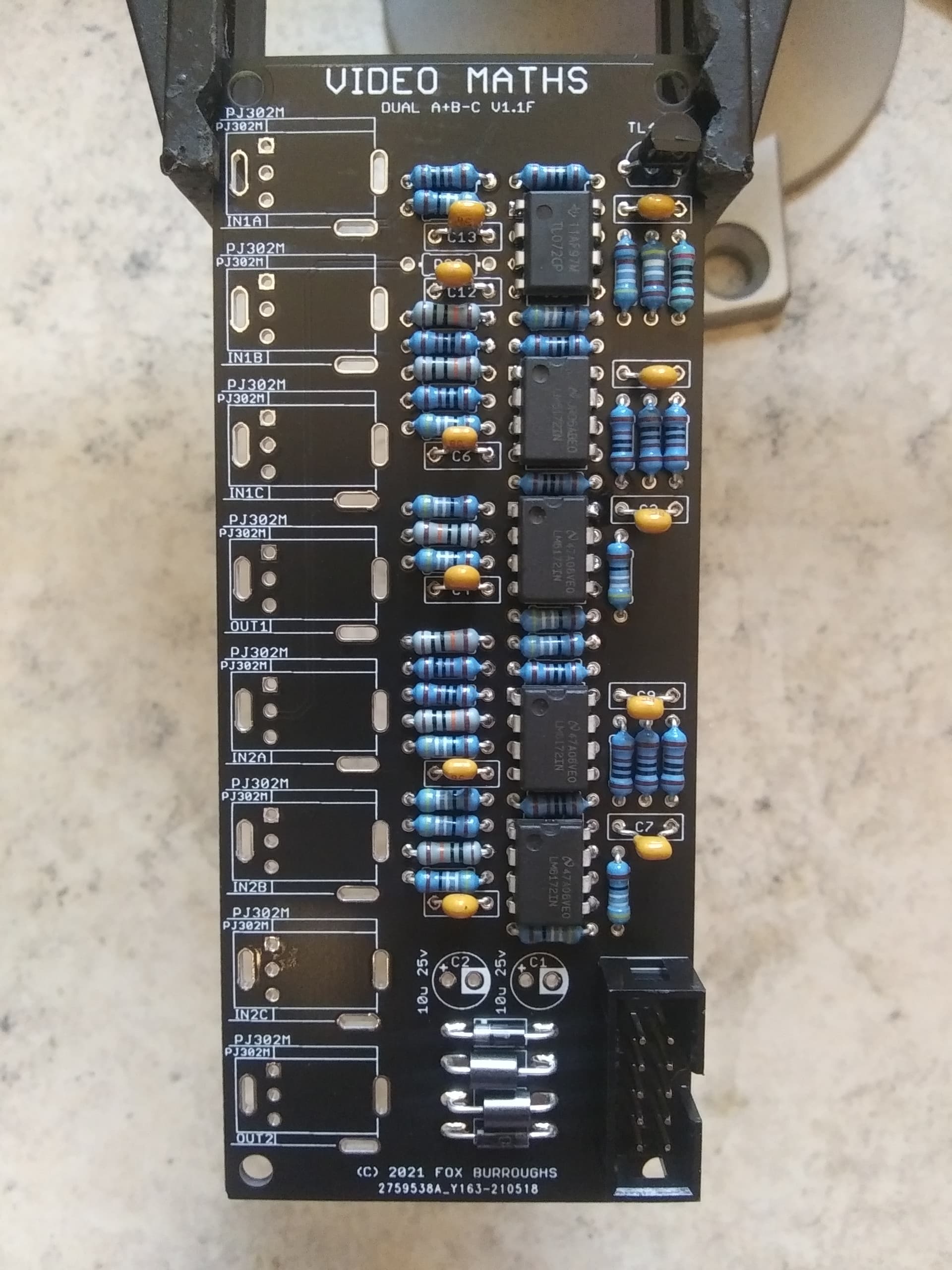
Step 13.
There are eight PJ302M jacks. Place each of them into the board and install the faceplate carefully. Finger-tighten a nut onto each jack and make sure they are lined up straight before soldering.
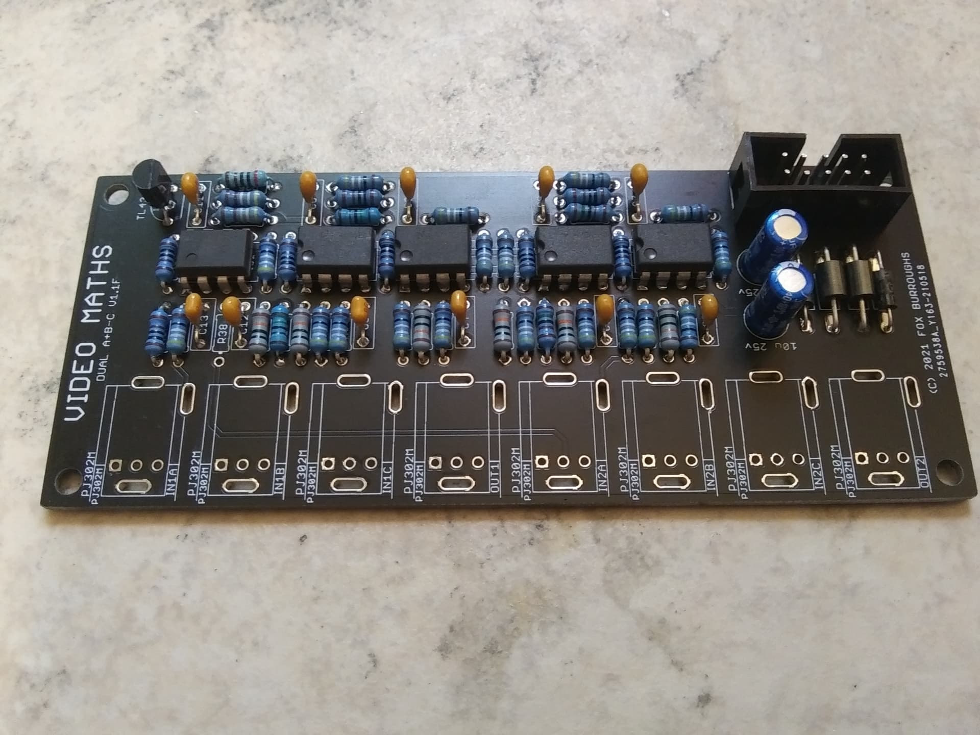
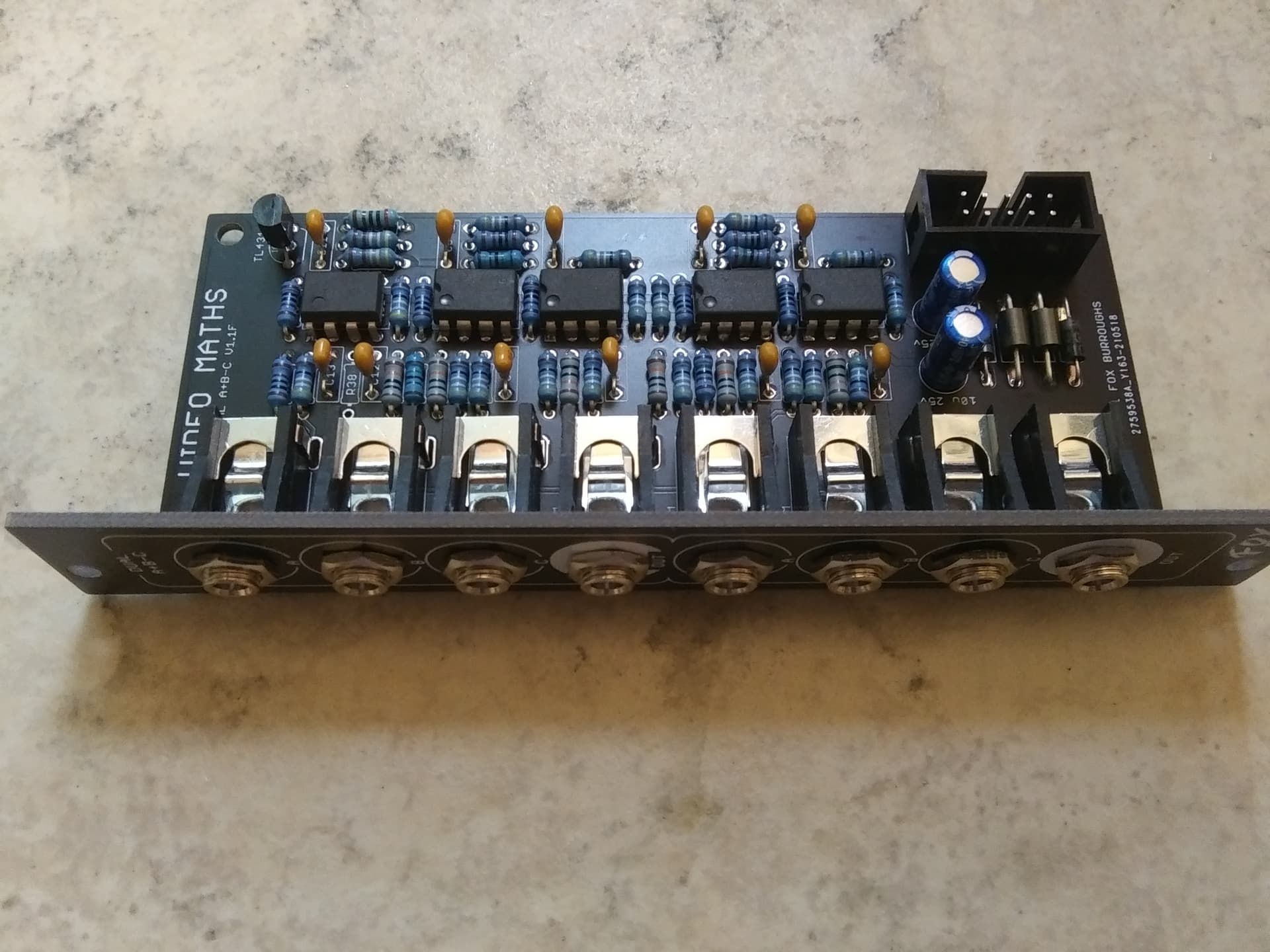
Step 14.
Finally, we will add the solder-jumpers to the bottom of the board. This configuration requires JP2 and JP4 to be soldered. Do not solder the others.
Clean up your board and test it out!
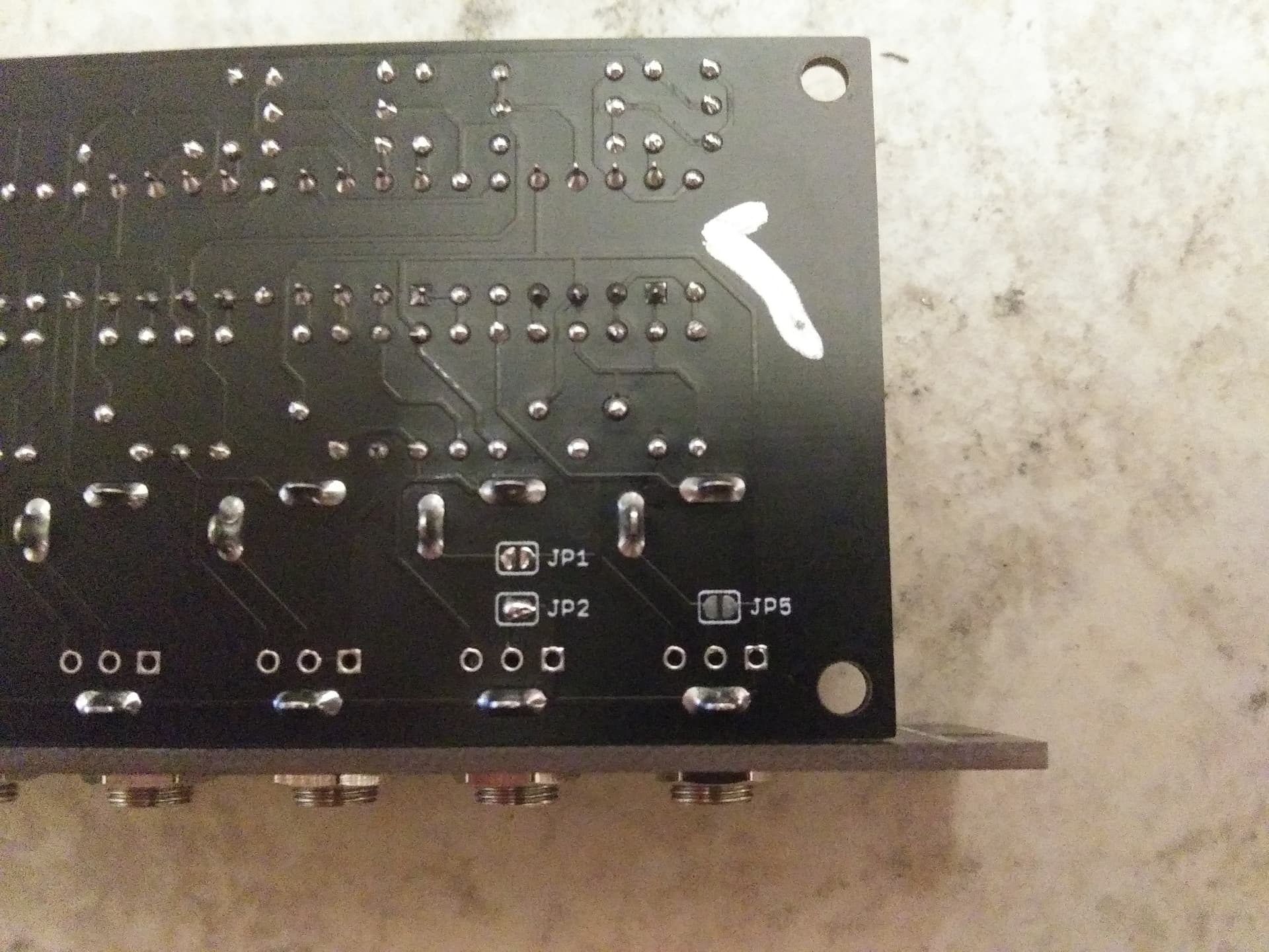
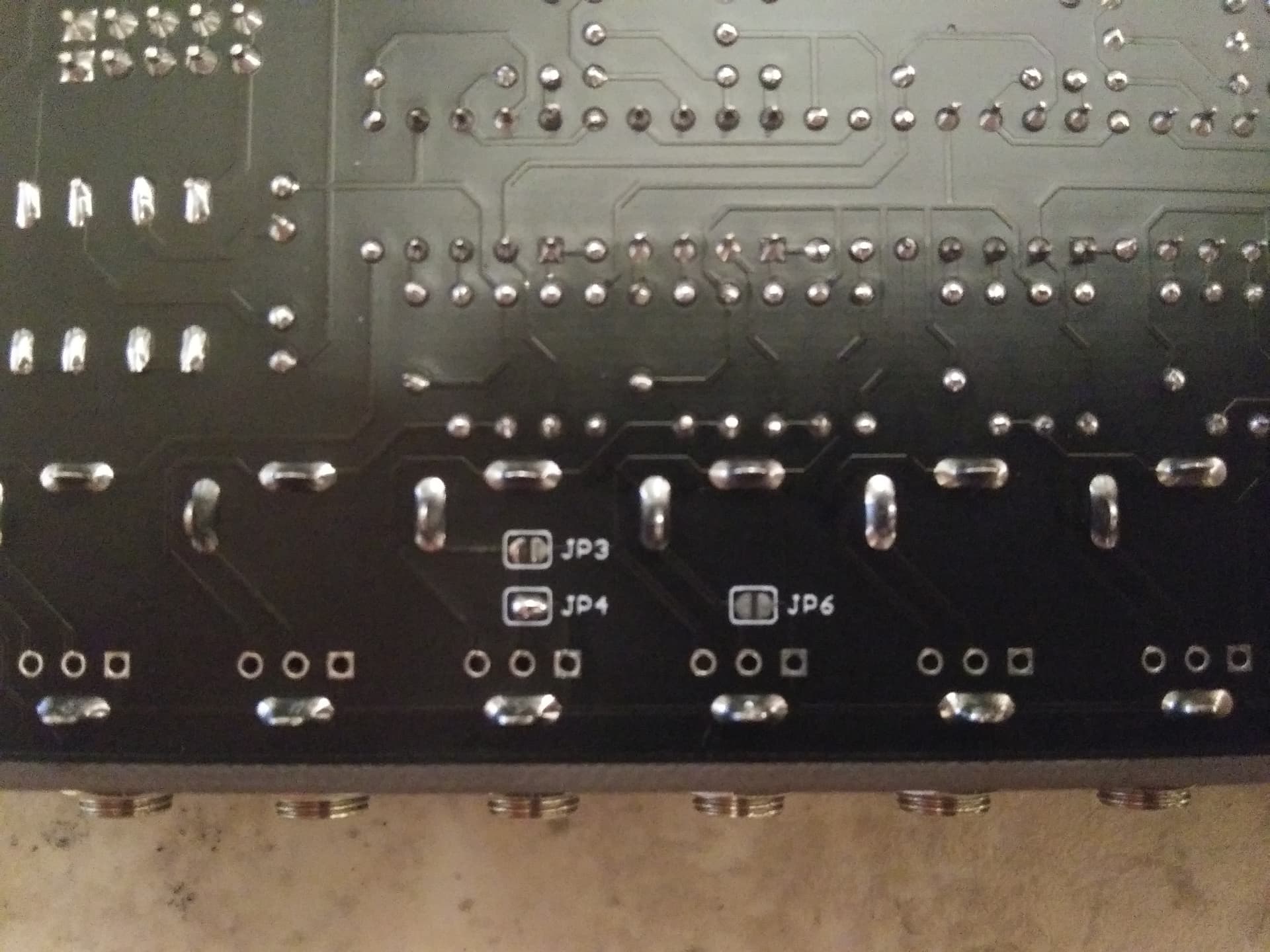
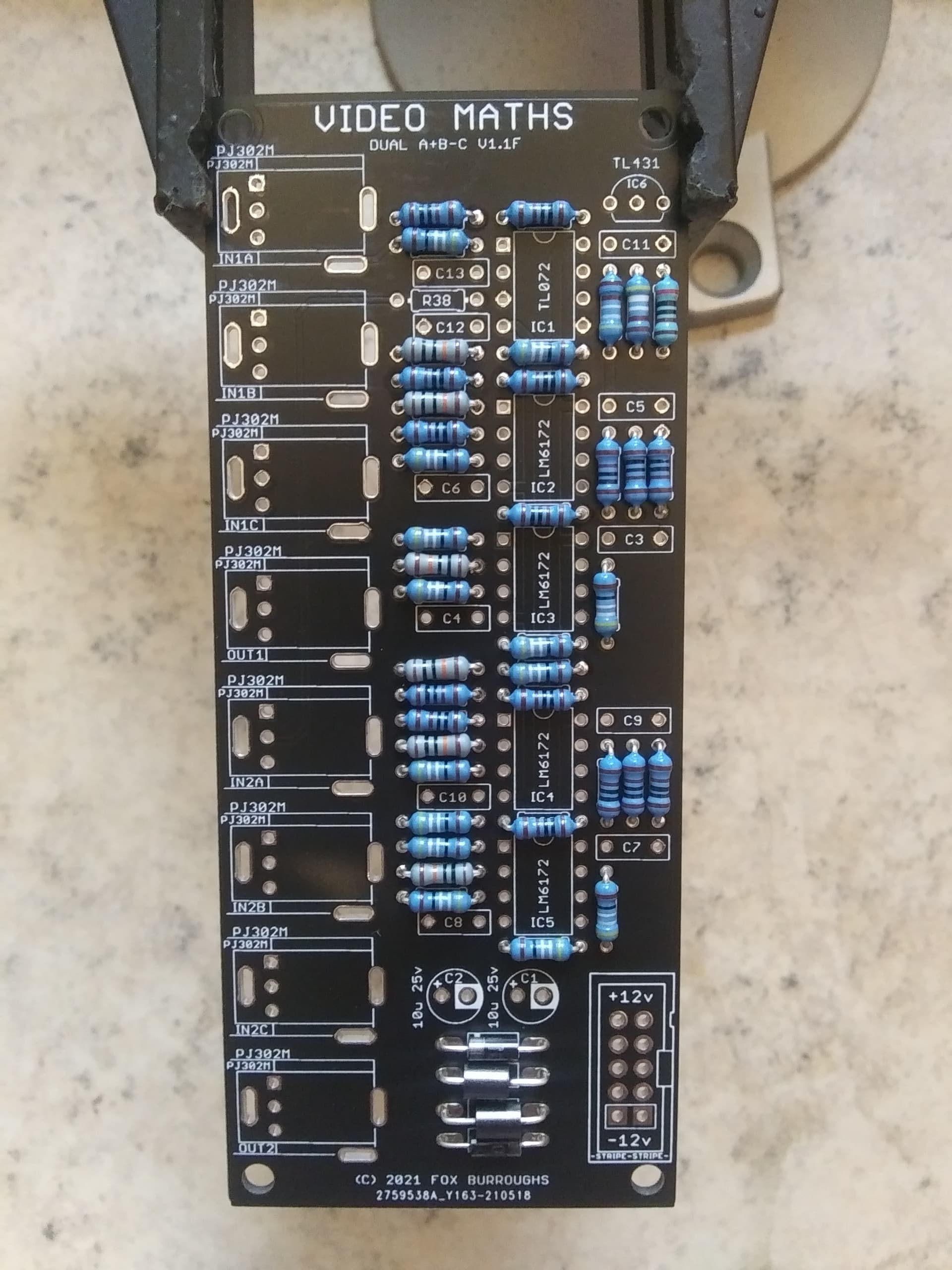
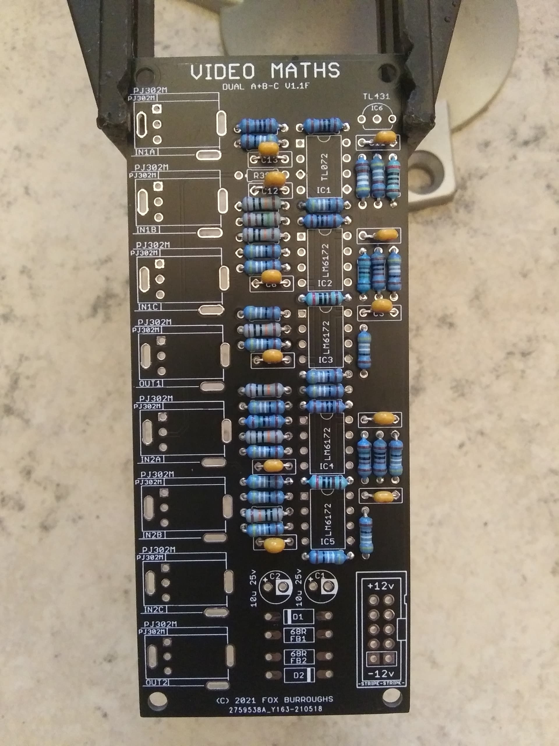
BOM for (A+B)/2-C configurationQtyValueParts210u/25v capacitorC1, C211100n capacitorC3, C4, C5, C6, C7, C8, C9, C10, C11, C12, C13110-Pin Box HeaderCONN921N4001 diodeD1, D2268R ferrite beadFB1, FB21TL072 ICIC14LM6172 ICIC2, IC3, IC4, IC51TL431IC68PJ302M jacksIN1A, IN1B, IN1C, IN2A, IN2B, IN2C, OUT1, OUT214499R resistorR4, R6, R8, R13, R15, R16, R20, R22, R24, R29, R31, R32, R39, R42161K resistorR5, R7, R9, R10, R11, R12, R14, R21, R23, R25, R26, R27, R28, R30, R36, R3712K resistorR3524.99K resistorR33, R346100K resistorR1, R2, R3, R17, R18, R192Solder JumperJP1, JP31PCB set-110-16 Power ribbon----5DNPR38, JP2, JP4, JP5, JP6*Solder jumpers are located on bottom-side of board.
*DNP means Do not populate.
*Unless specified differently, All resistors are always Metal Film type, 1/4W, 1% tolerance.
Build Guide for (A+B)/2-CStep 0.
Using a PCB vice will improve your DIY experience immensely.
Step 1.
First, populate the 499R resistors. There are fourteen of them: R4, R6, R8, R13, R15, R16, R20, R22, R24, R29, R31, R32, R39, R42
Step 2.
Next populate all sixteen 1K resistors: R5, R7, R9, R10, R11, R12, R14, R21, R23, R25, R26, R27, R28, R30, R36, R37
Step 3.
There is only one 2K resistor needed: R35
Step 4.
Beside the resistor above, there are two 4.99K resistors: R33 and R34.
Step 5.
Finally, there are six 100K resistors: R1, R2, R3, R17, R18, R19. I prefer to solder all of the resistors at once.
Step 6.
Now populate both diodes and ferrite beads taking note of the diode’s polarity.
Step 7.
There are eleven 100nF caps to solder: C3, C4, C5, C6, C7, C8, C9, C10, C11, C12, C13
Step 8.
Now you may move on to the ICs. Start by soldering the TL431 in place, IC6. The first 8-pin op amp is a TL072, IC1. And finally you may solder IC2-IC5, all if which are LM6172. Make sure pin one for each of these is lined up correctly.
Step 9.
Then you may populate the 10-pin power header and both electrolytic caps. The power connector has a notch which needs to be lined up as shown on the silk screen.
Take special note of the polarity of the caps as well. Line up the stripe on each cap (negative) with the circled vias on the silkscreen.
Step 10.
There are eight PJ302M jacks. Place each of them into the board and install the faceplate carefully. Finger-tighten a nut onto each jack and make sure they are lined up straight before soldering.
Step 11.
Finally the last step is to add solder blobs to the jumpers on the bottom of the board. For this configuration, solder JP1 and JP3.
Thats it. Clean up your board and test!
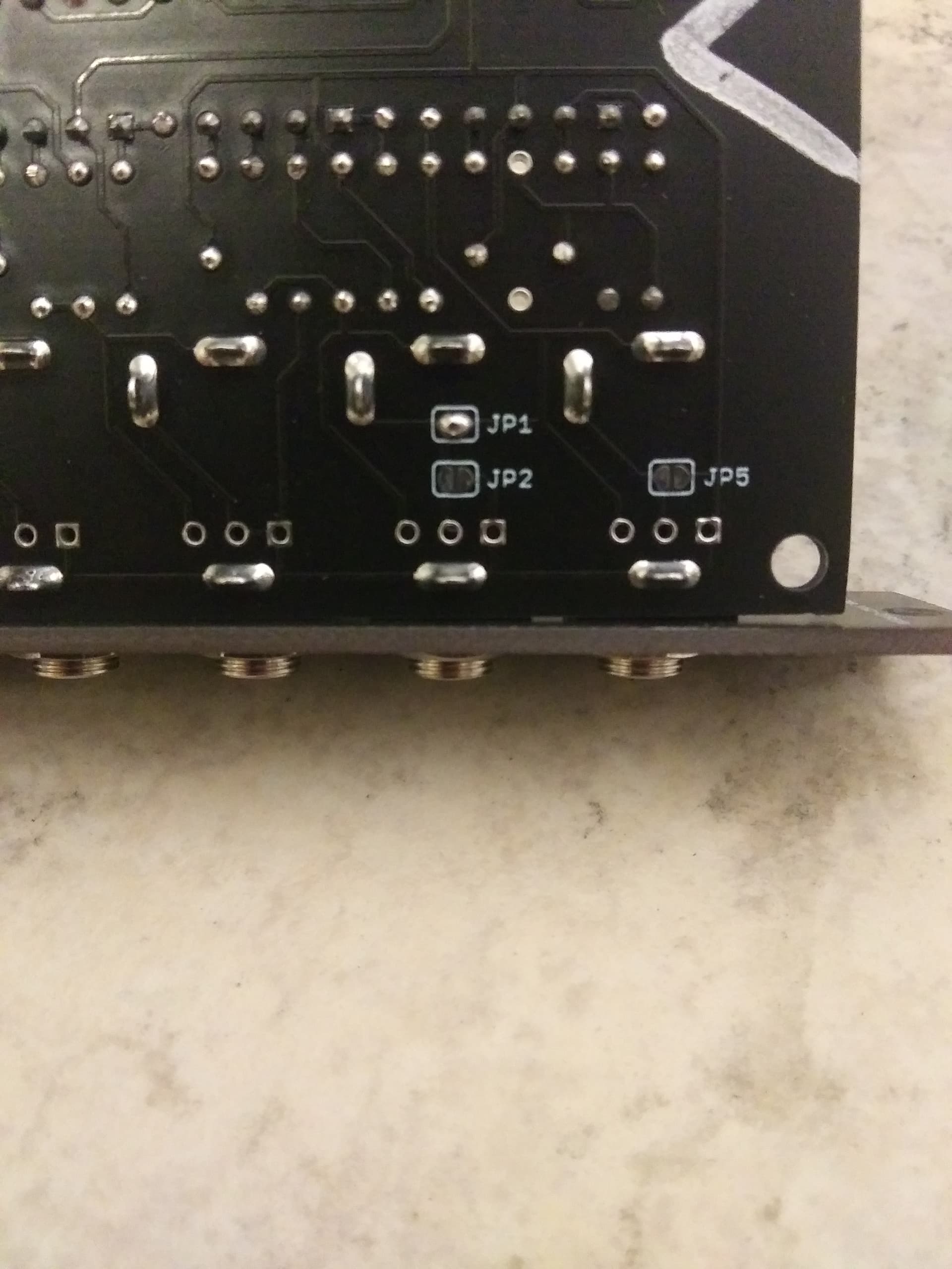
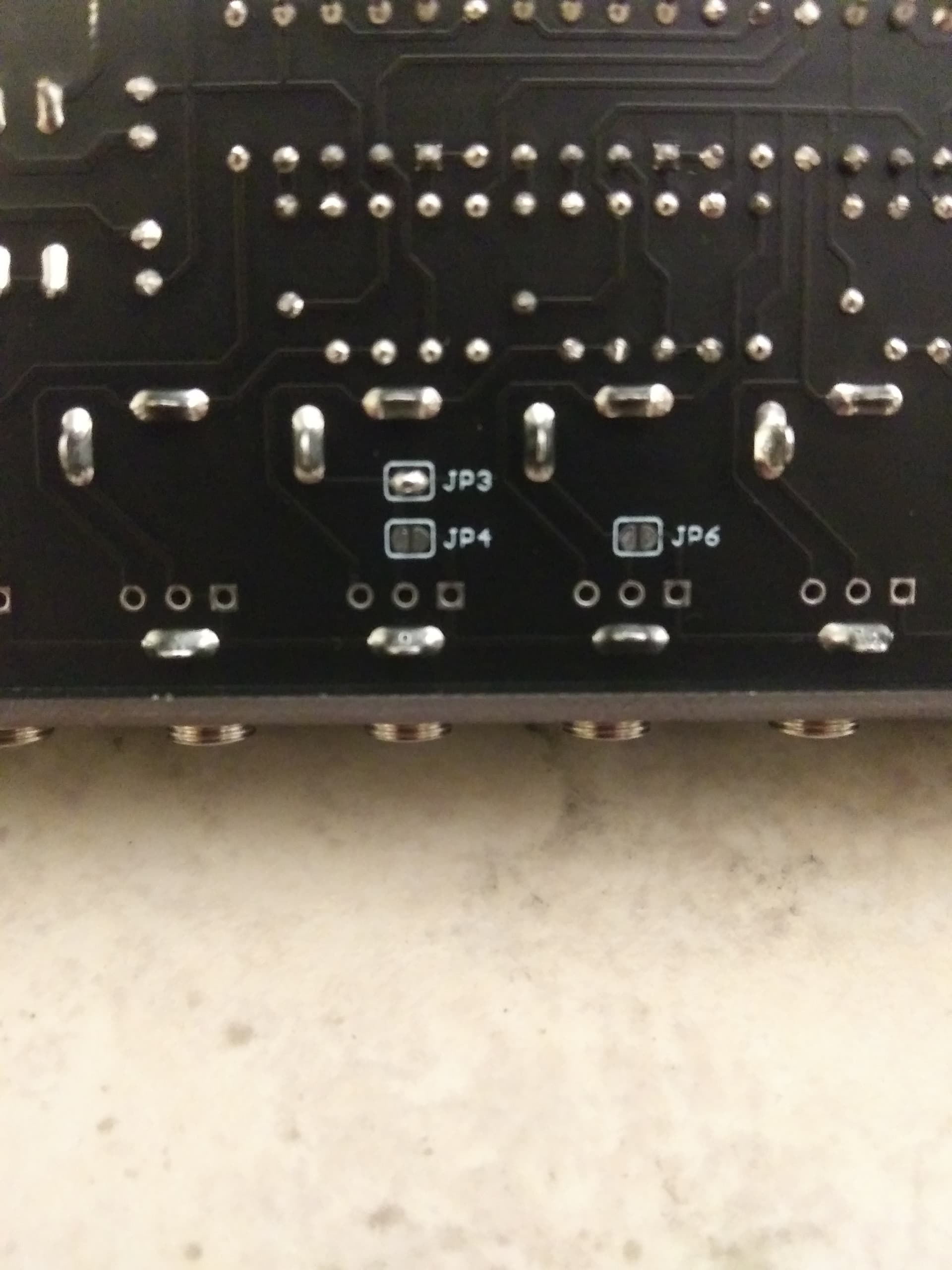
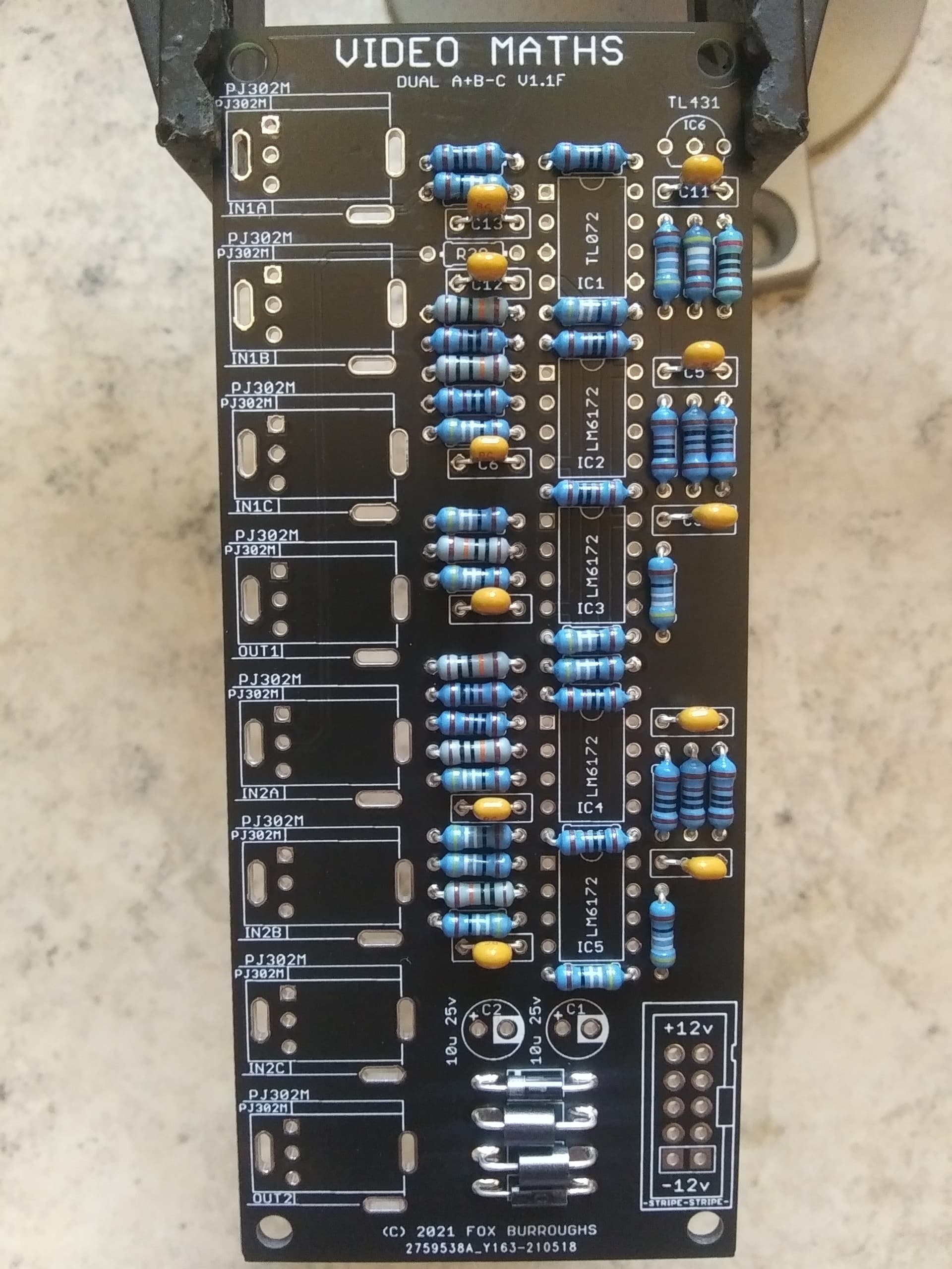
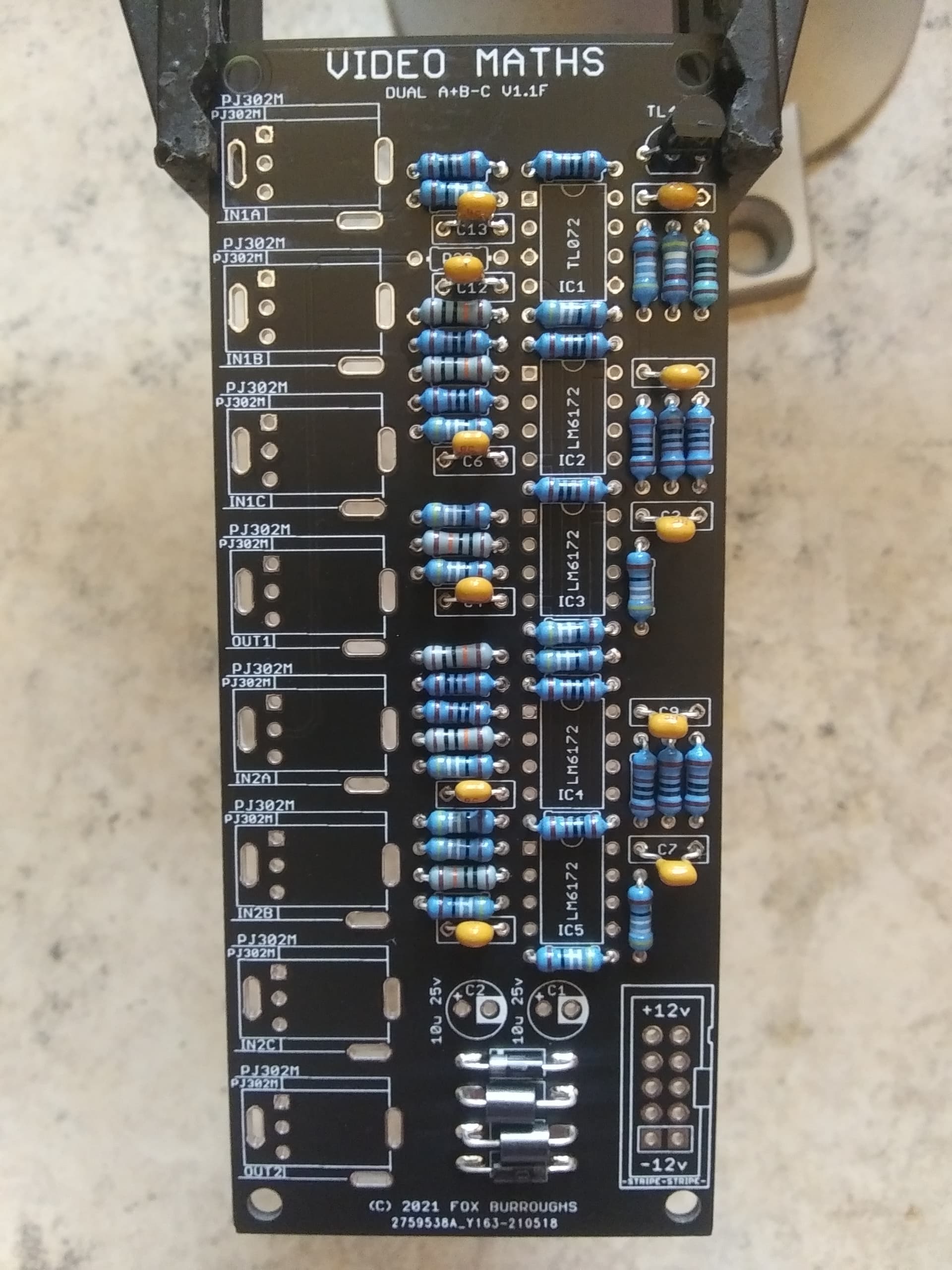
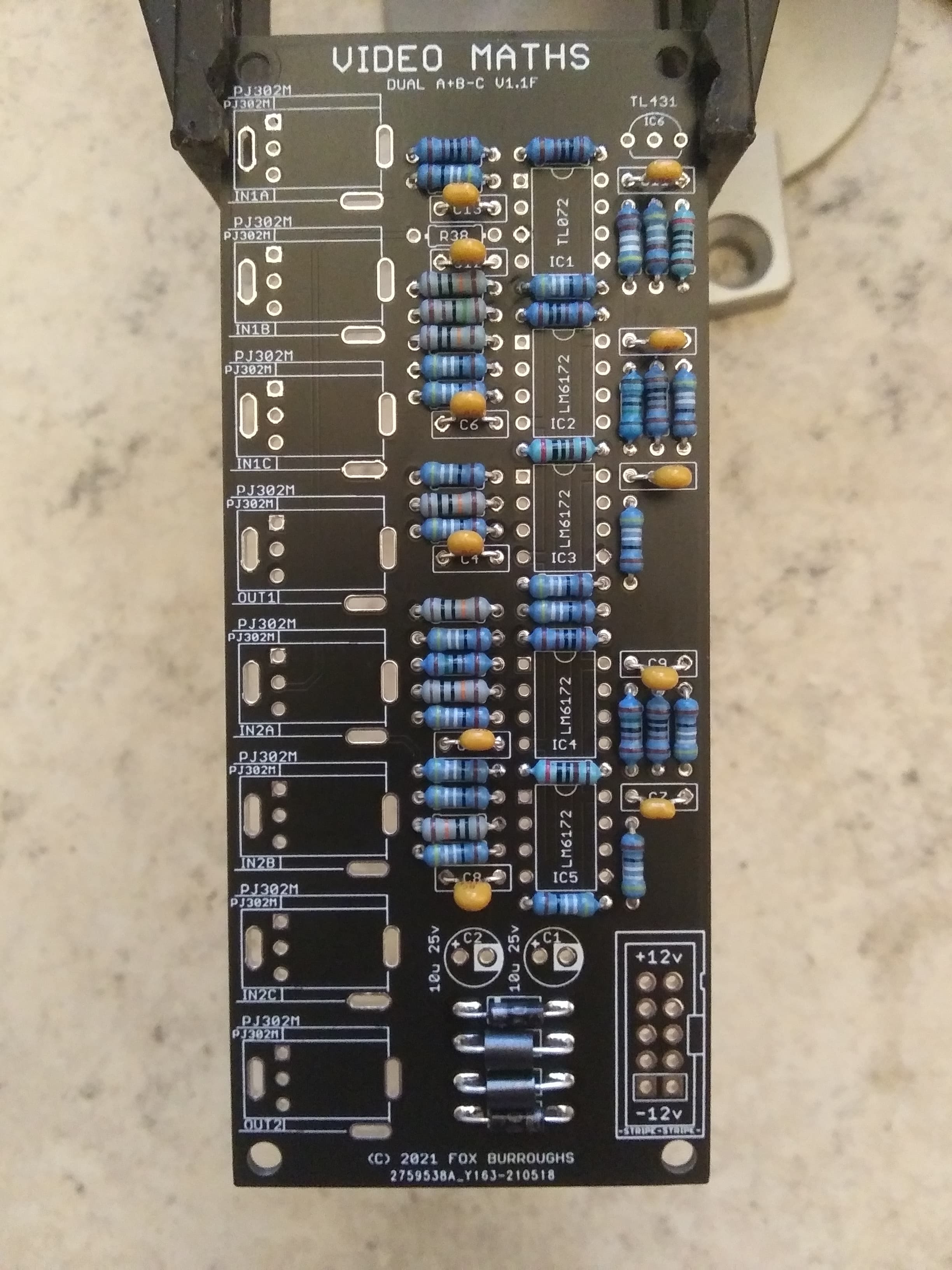
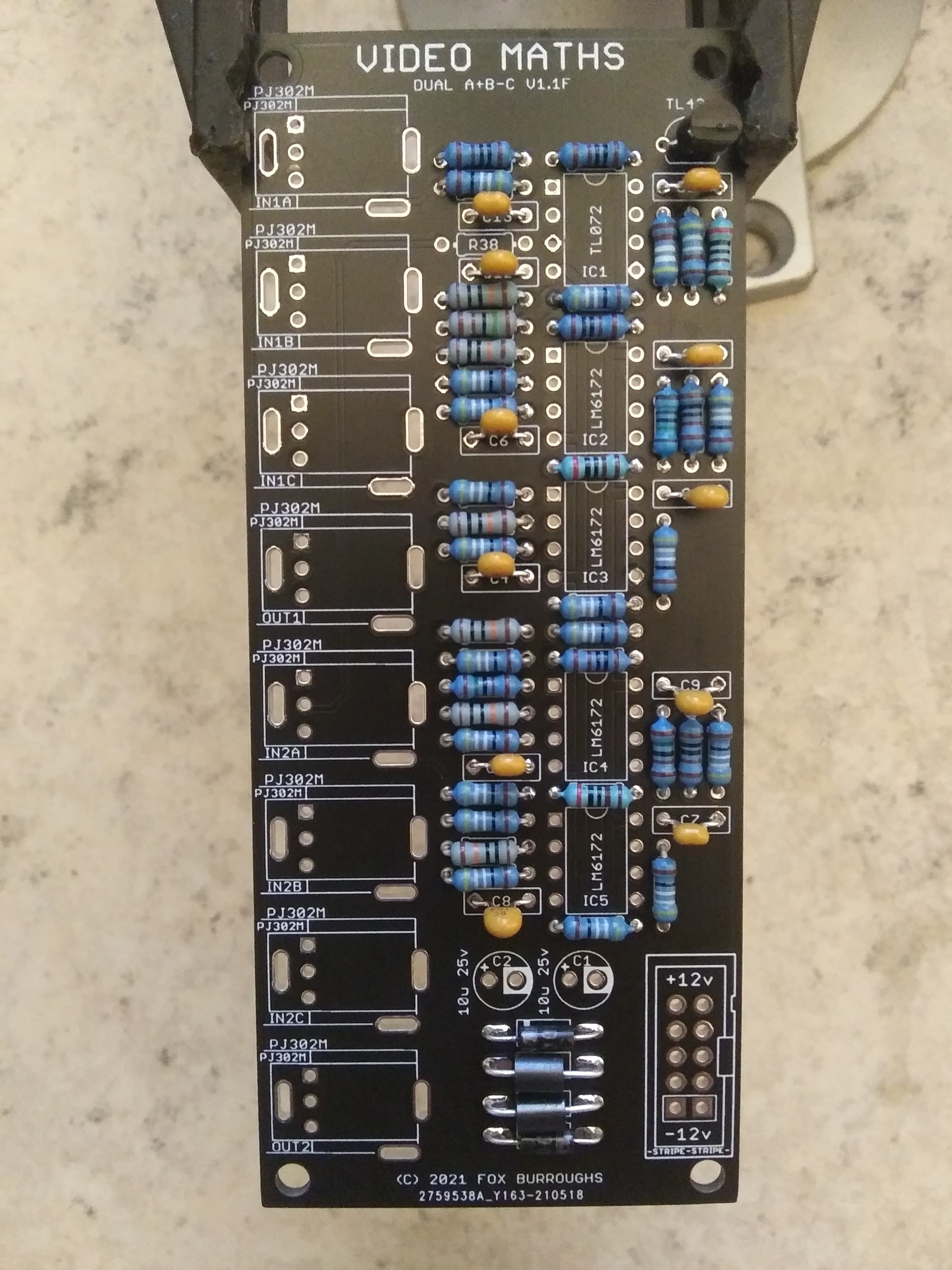
BOM for (A+B-C)/2 configurationQtyValueParts110-Pin Box Header CONN911100nC3, C4, C5, C6, C7, C8, C9, C10, C11, C12, C13210u 25vC1, C218499RR4, R5, R6, R7, R8, R13, R15, R16, R20, R21, R22, R23, R24, R29, R31, R32, R39, R4261KR11, R12, R27, R28, R36, R3741.5KR9, R10, R25, R2632KR14, R30, R3524.99KR33, R346100KR1, R2, R3, R17, R18, R1921N4001D1, D2268RFB1, FB24LM6172IC2, IC3, IC4, IC58PJ302MIN1A, IN1B, IN1C, IN2A, IN2B, IN2C, OUT1, OUT21TL072IC11TL431IC62Solder JumperJP1, JP3---5DNPJP2, JP4, JP5, JP6, R38*Solder jumpers are located on bottom-side of board.
*DNP means Do not populate.
*Unless specified differently, All resistors are always Metal Film type, 1/4W, 1% tolerance.
Build Guide for (A+B-C)/2Step 0.
Using a PCB vice will improve your DIY experience immensely.
Step 1.
Start by populating the 499R resistors. There are 18 of them: R4, R5, R6, R7, R8, R13, R15, R16, R20, R21, R22, R23, R24, R29, R31, R32, R39, R42.
Step 2.
Next, populate the six 1K resistors: R11, R12, R27, R28, R36, R37.
Step 3.
Now populate all four 1.5K resistors: R9, R10, R25, R26.
Step 4.
Next populate all three 2K resistors: R14, R30, R35.
Step 5.
Finally, populate all six 100K resistors: R1, R2, R3, R17, R18, R19.
Step 6.
Now populate all eleven 100nF capacitors.
Step 7.
At the bottom of the board, populate both diodes and ferrite beads. Take note of the diodes polarity stripes. These line up with the lines on the pcb.
Step 8.
In the top right, populate the TL431.
Step 9.
The first op amp, IC1; is a TL072. Make sure pin 1 is inserted into the square via.
Step 10.
The other four op amps are all LM6172’s. Make sure pin 1 of each of them is inserted into the square vias.
Step 11.
Now populate the 10-pin shrouded header. The notch faces outward.
Step 12.
Now populate both 10uF electrolytic capacitors. These are polarized, so line up the stripe on the cap with the circled-via on the pcb.
Step 13.
There are eight PJ302M jacks. Place each of them into the board and install the faceplate carefully. Finger-tighten a nut onto each jack and make sure they are lined up straight before soldering.
Step 14.
Finally the last step is to add solder blobs to the jumpers on the bottom of the board. For this configuration, solder JP1 and JP3.
Thats it. Clean up your board and test!
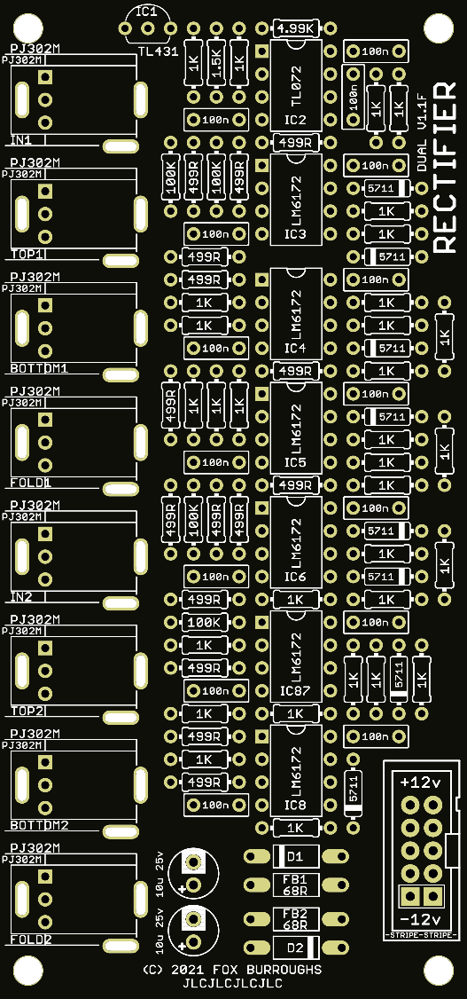
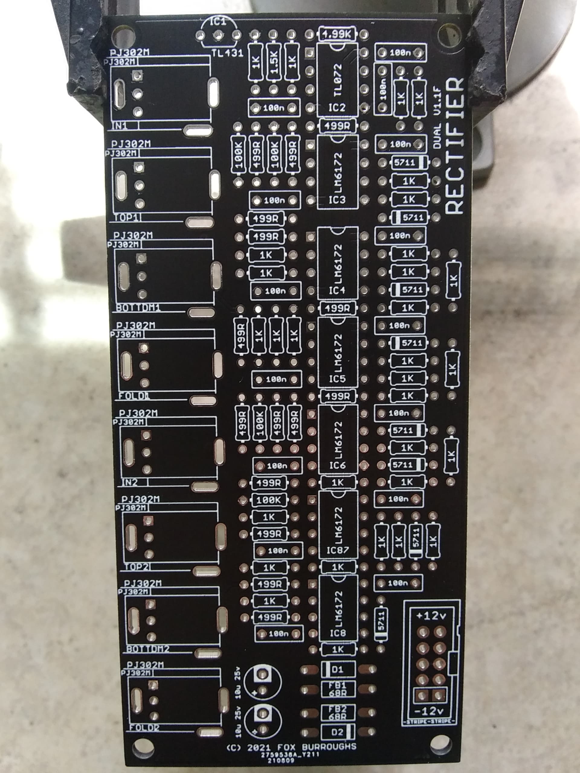
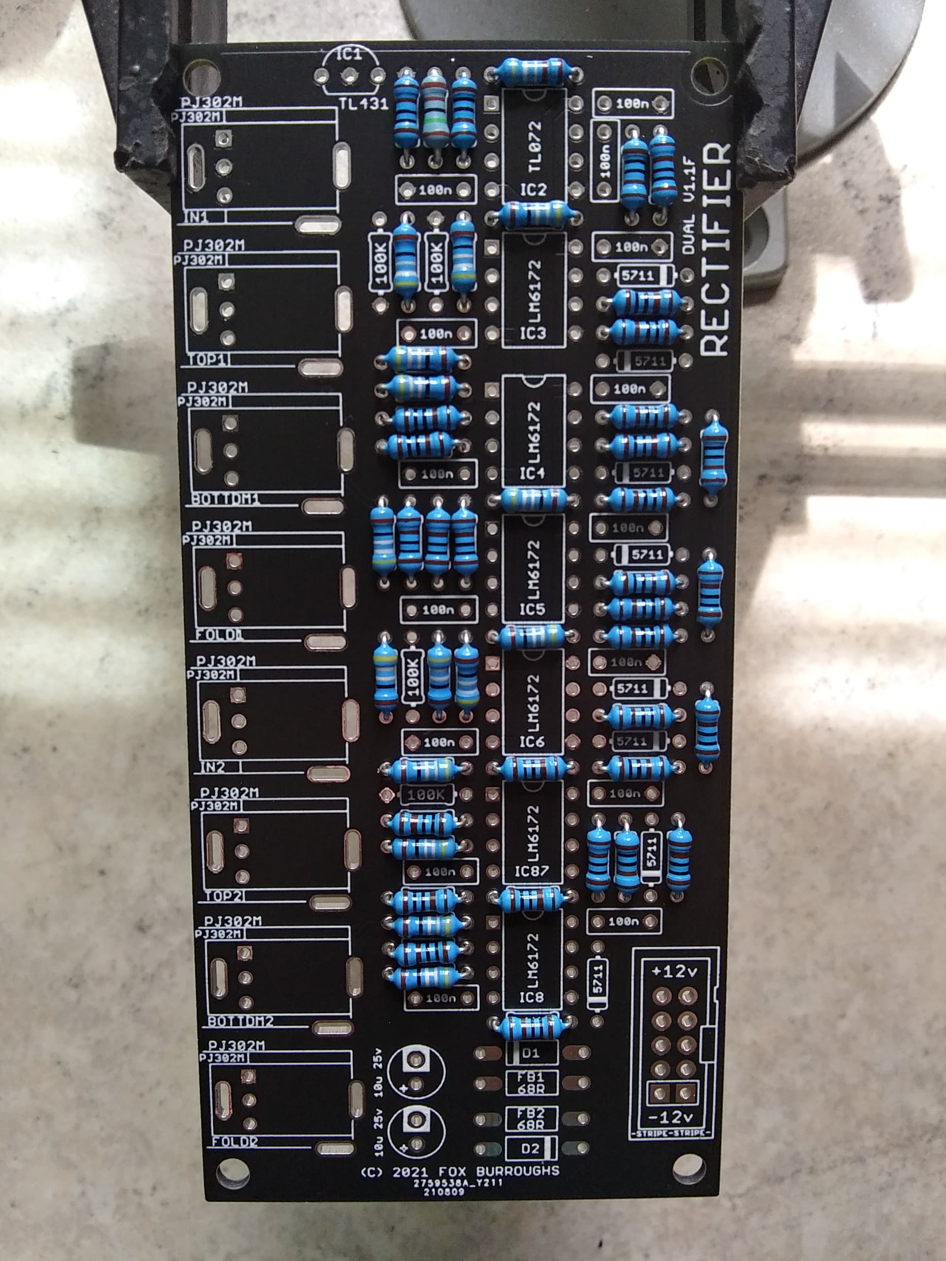
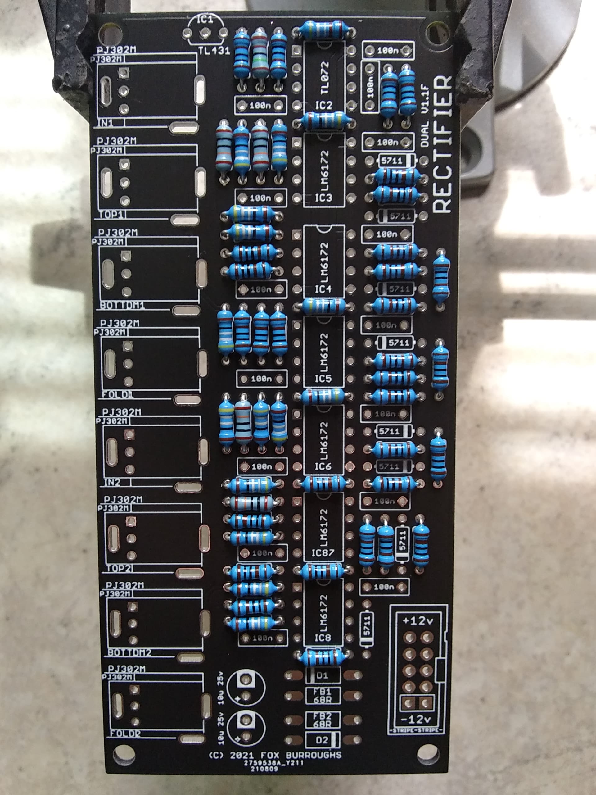
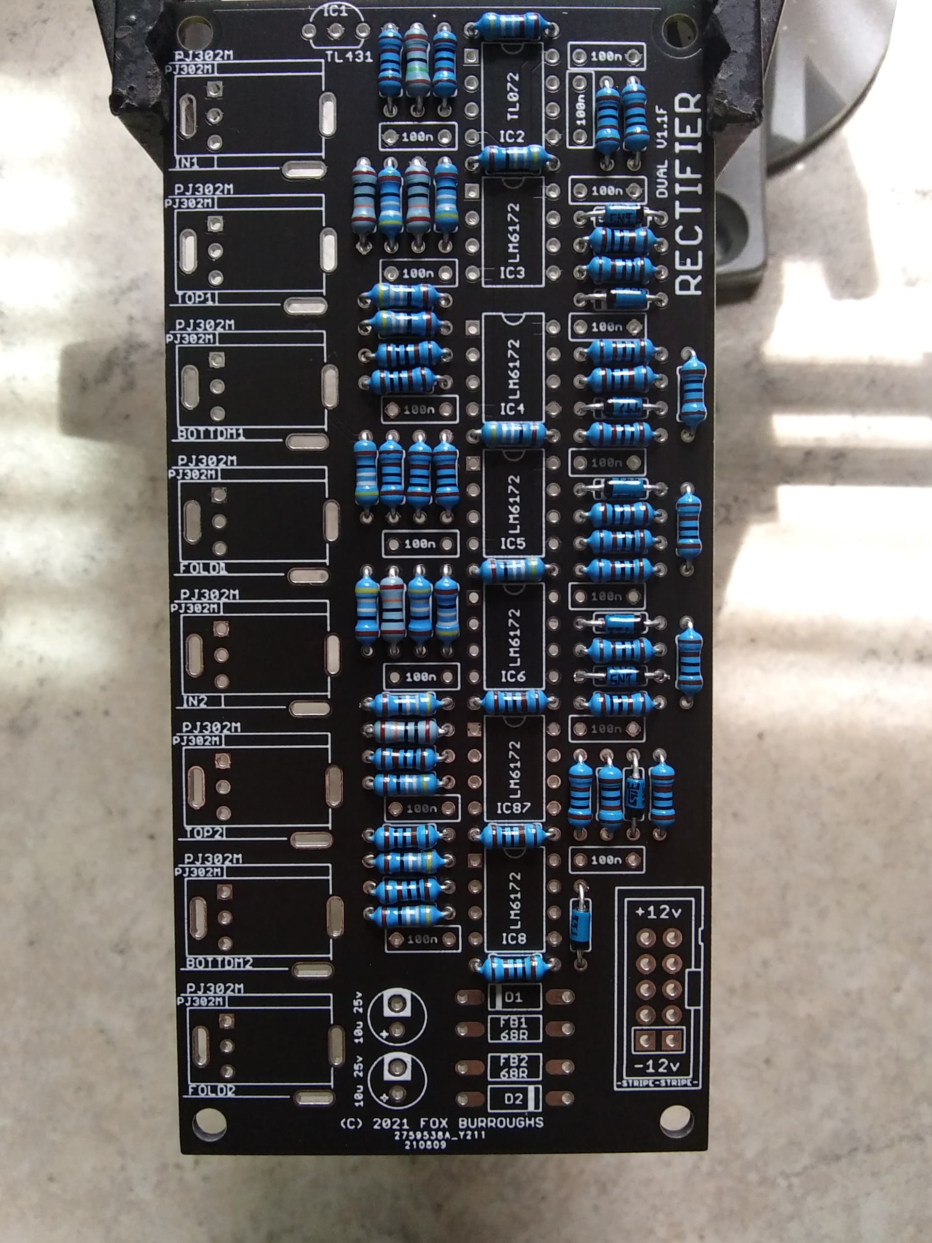
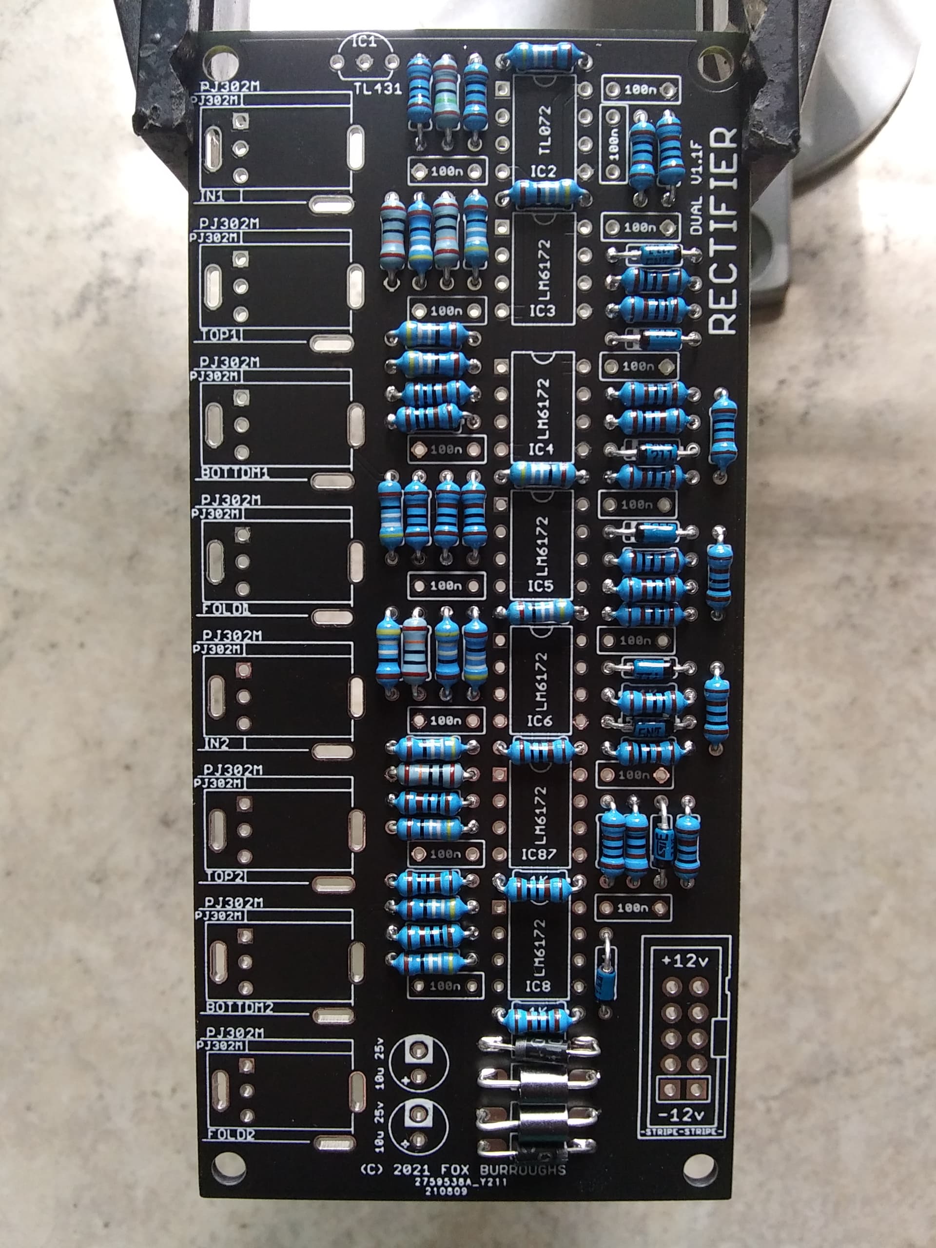
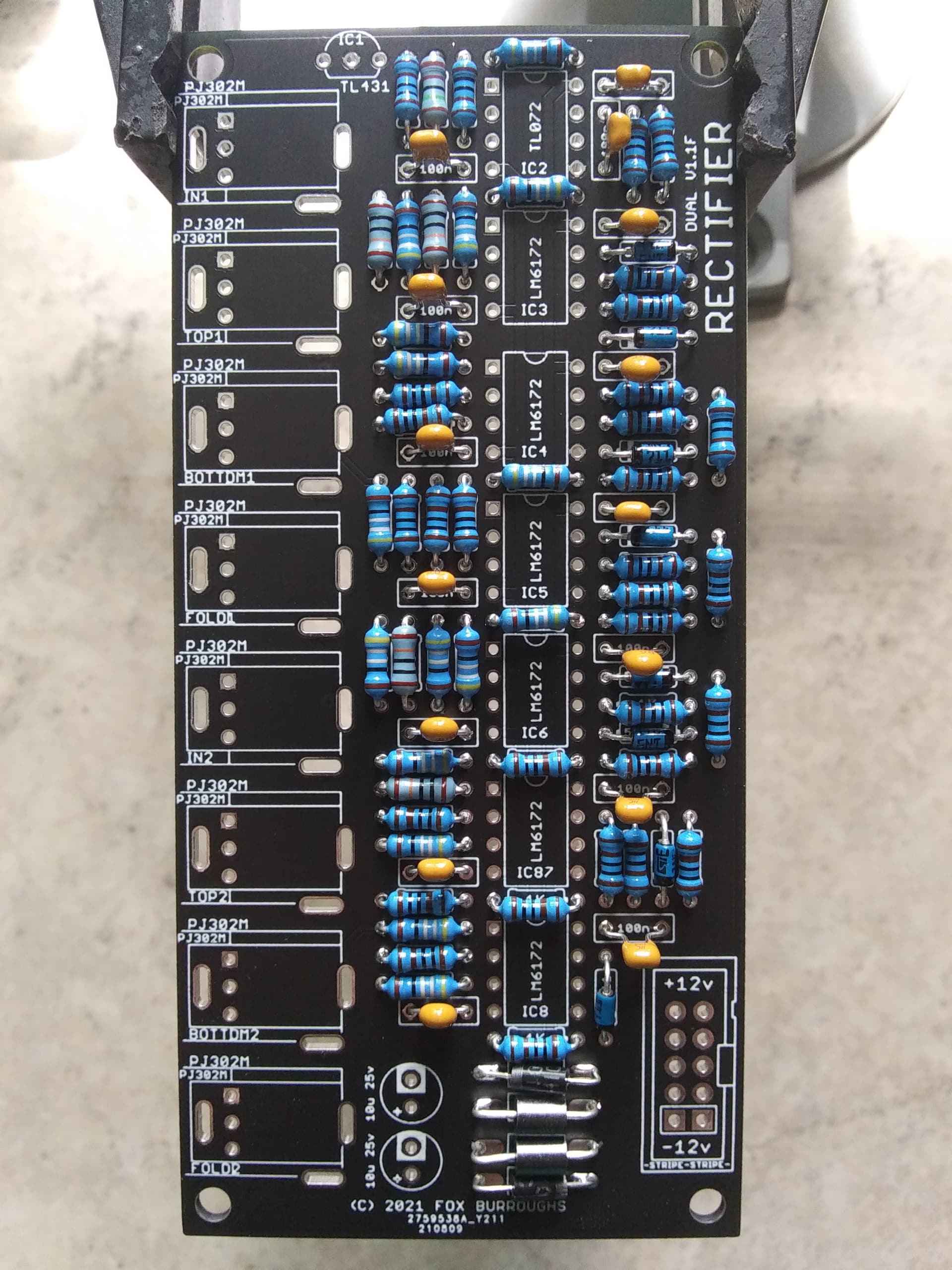
BOM for RectifierQtyValueParts11.5K resistorR2110-Pin Box HeaderJ94100K resistorR6, R8, R30, R3215100n capacitorC3, C4, C5, C6, C7, C8, C9, C10, C11, C12, C13, C14, C15, C16, C17210u 25v capacitorC1, C2311K resistorR3, R4, R5, R10, R12, R13, R14, R15, R16, R17, R18, R20, R21, R22, R23, R24, R25, R34, R36, R37, R38, R39, R40, R41, R42, R44, R45, R46, R47, R48, R4921N4001 diodeD1, D214.99K resistorR115499R resistorR7, R9, R11, R19, R26, R27, R28, R29, R31, R33, R35, R43, R50, R51, R5281n5711 diodeD3, D4, D5, D6, D7, D8, D9, D10268R ferrite beadFB1, FB26LM6172 op ampIC3, IC4, IC5, IC6, IC8, IC878PJ302M jackBOTTOM1, BOTTOM2, FOLD1, FOLD2, IN1, IN2, TOP1, TOP21TL072 op ampIC21TL431 referenceIC18nuts-1Pcb set-110-16 ribbon cable- Build Guide for RectifierStep 0.
Using a PCB vice will improve your DIY experience immensely. I’ve been using the same Panavise Jr. since 2014.
Step 1.
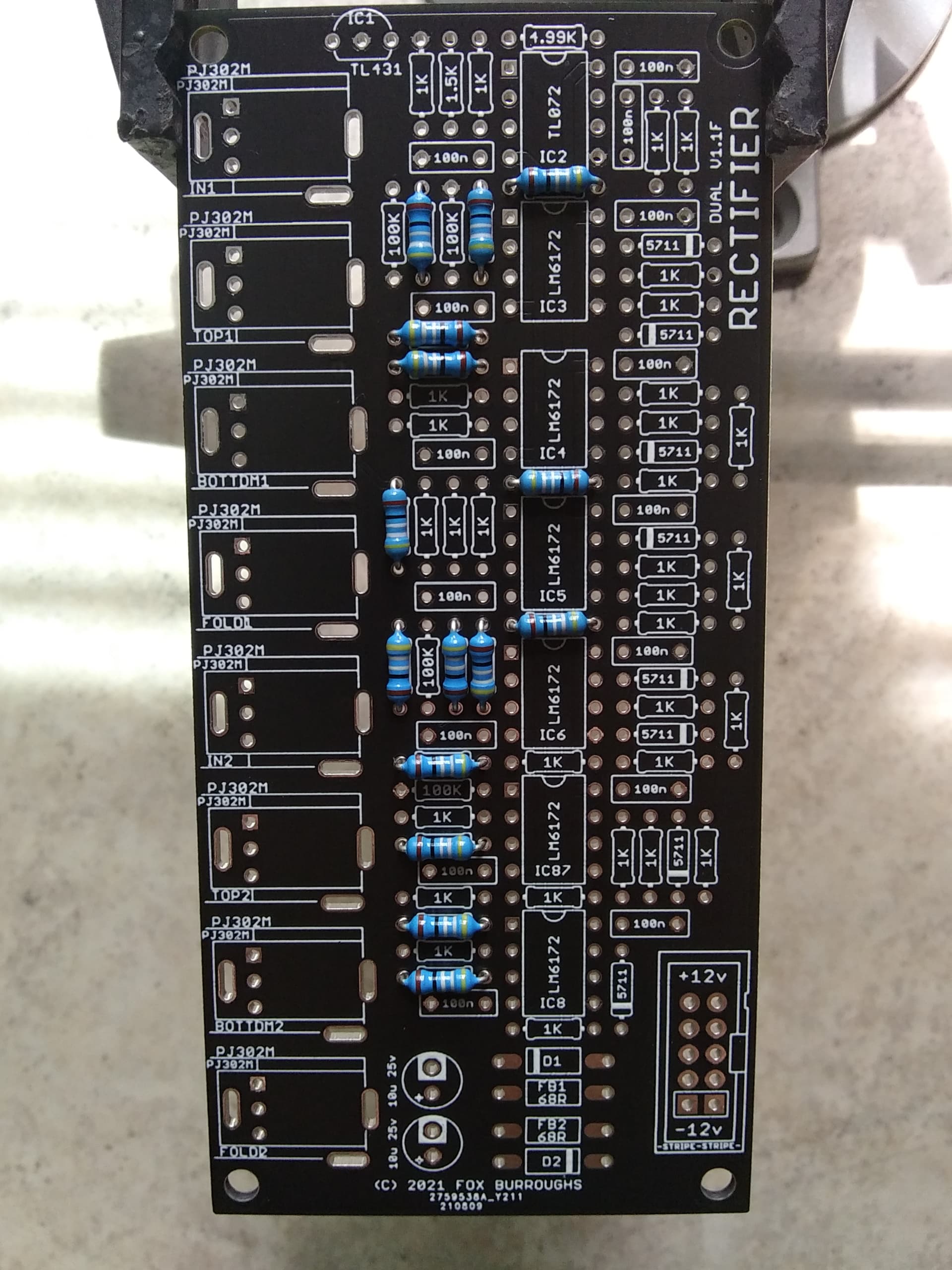
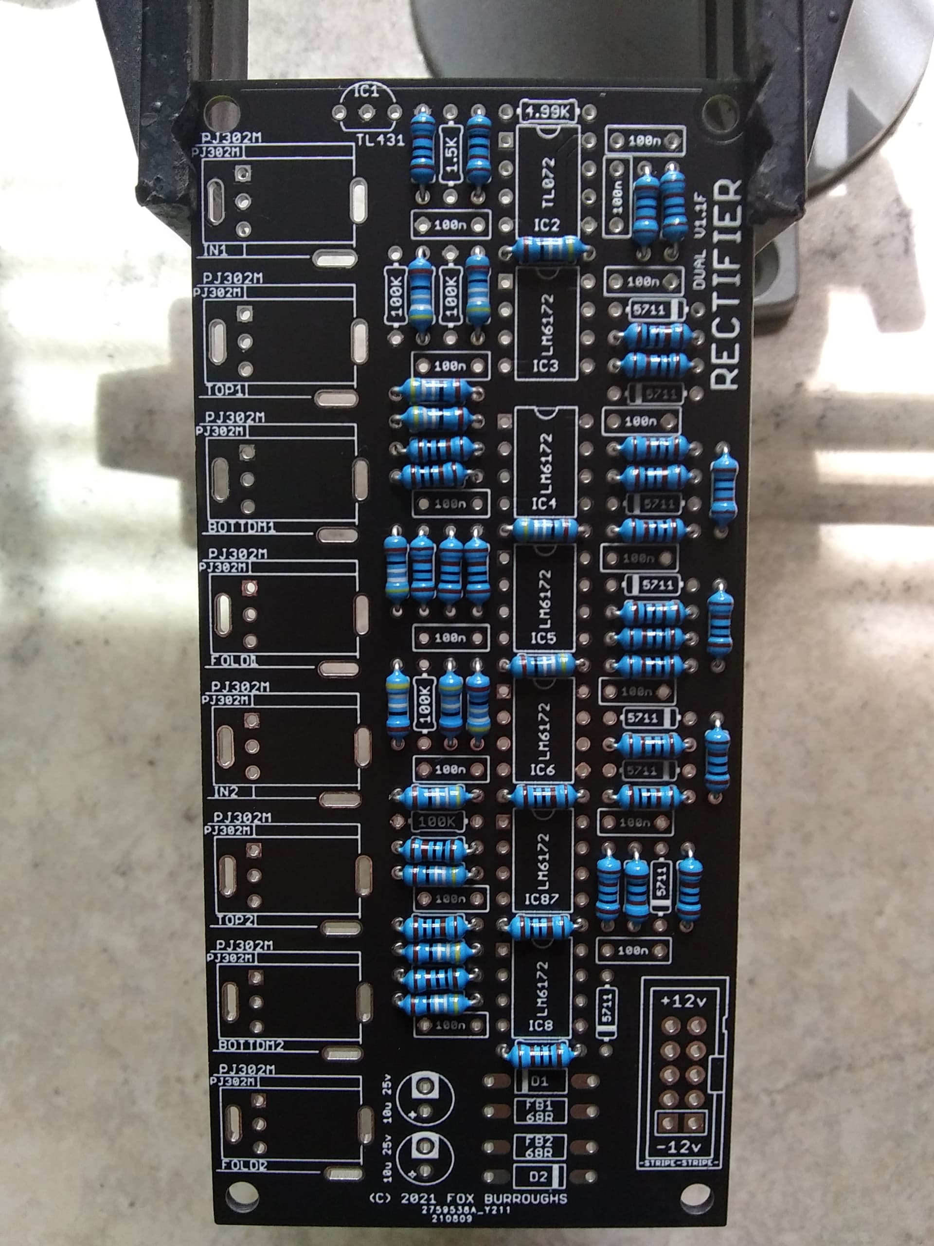
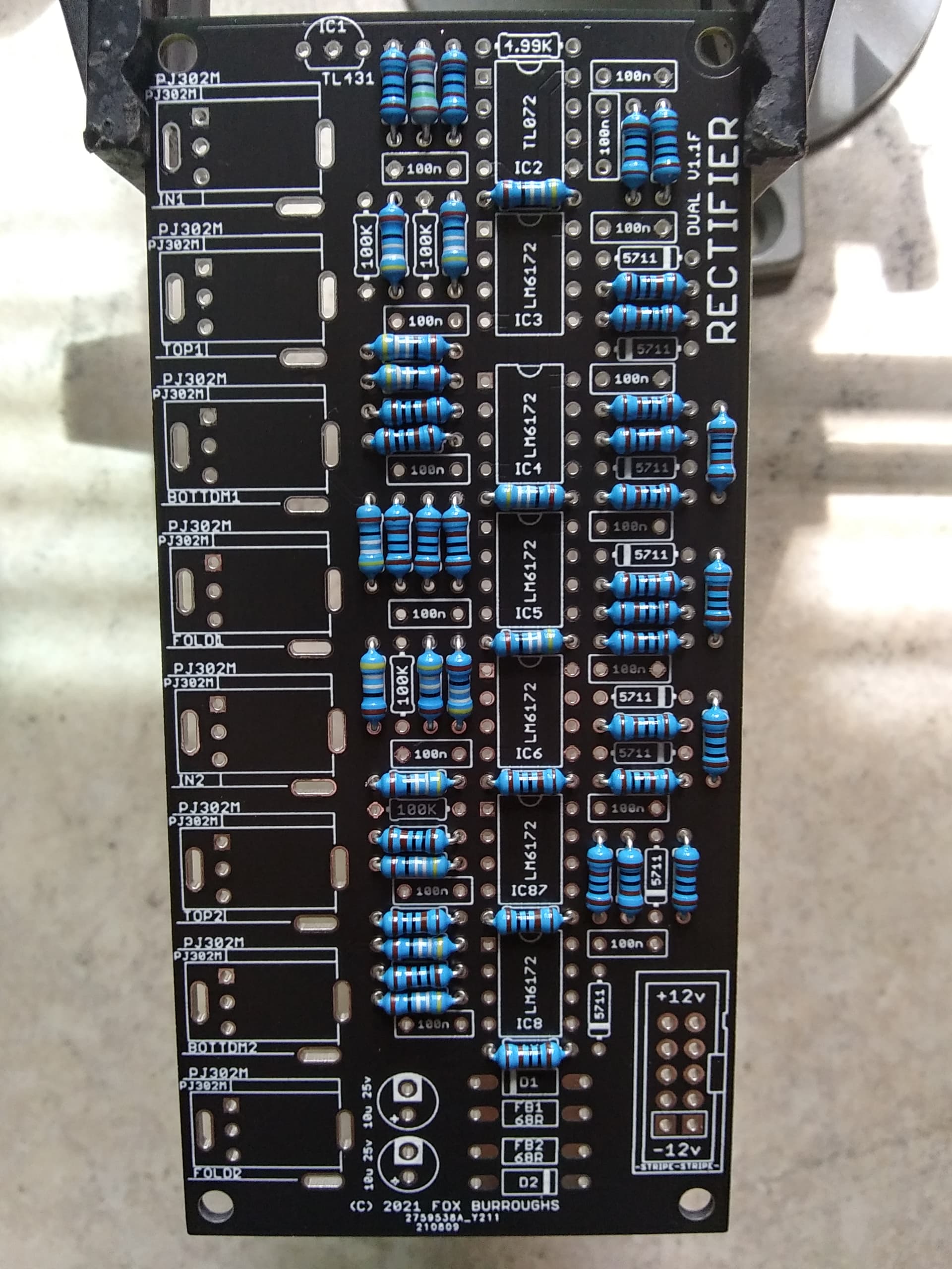
Start with the fifteen 499 ohm resistors.
I prefer to populate all of the resistors at once, and then solder them in place.
Step 2.
Next we will populate the 1K ohm resistors. There are a whopping 31 of them!
Step 3.
At the top, there is a single 4.99K ohm resistor and a single 1.5K ohm resistor. Populate both of them in their respective locations.
Step 4.
Next, populate the 100K ohm resistors. There are only six.
Step 5.
Now we have to add the 1n5711 diodes. Take note, these are polarized. Make sure the stripe on the diode matches the same direction as the stripe on the PCB. There are 8 diodes.
At this point, I carefully flip the board over onto my workspace and solder each leg then clip them all.
Step 6.
Now we can add both ferrite beads and both protection diodes. The ferrite is not polarized, but the diodes are. Line up your diodes properly and then solder all four parts in place. Clip the legs.
Step 7.
Now we can add all fifteen of the 100nF caps. Solder and clip.
Step 8.
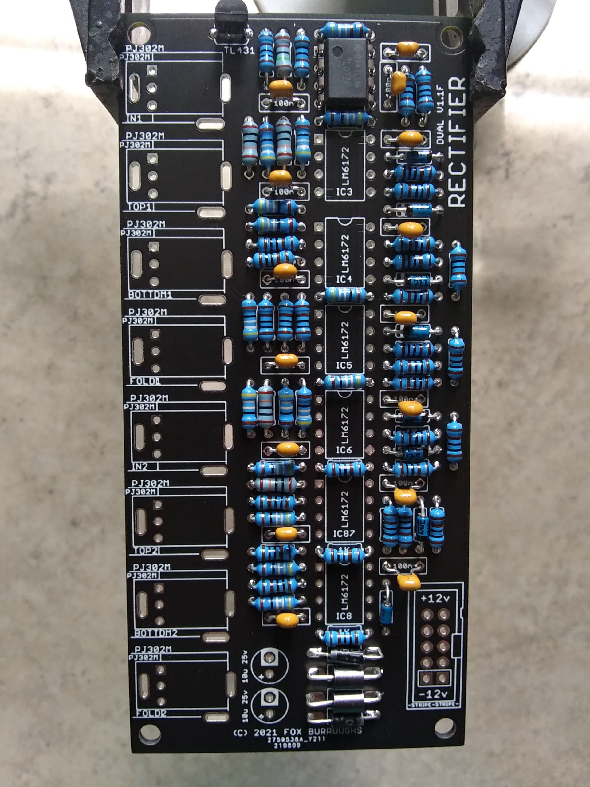
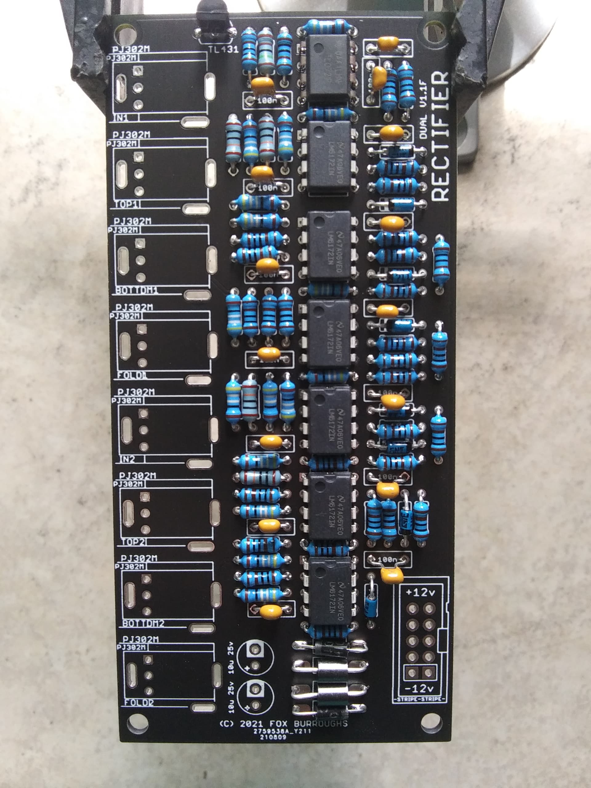
Now place your TL431 voltage reference. It is located at the top of the board.
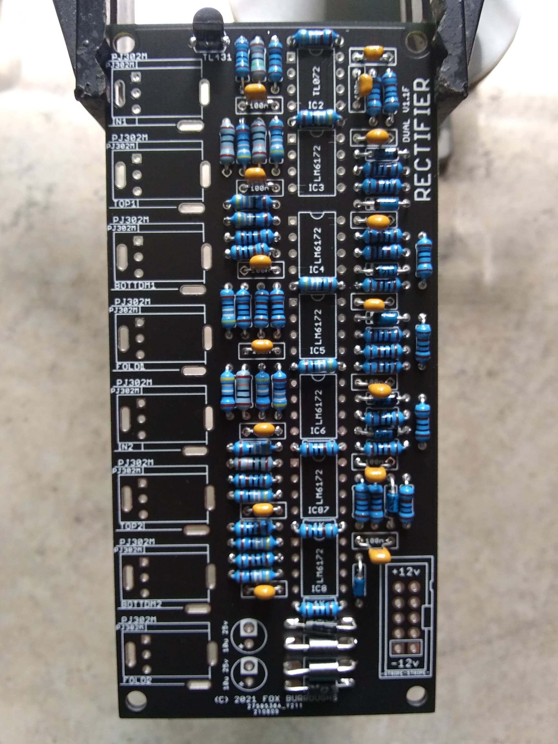
Step 9.
Here we will add all of our op amps. The top-most IC is a single TL072 while the remaining six are all LM6172’s. Make sure pin 1 of each IC is placed into the square hole.
Step 10.
Here we will add the 10-pin box header.
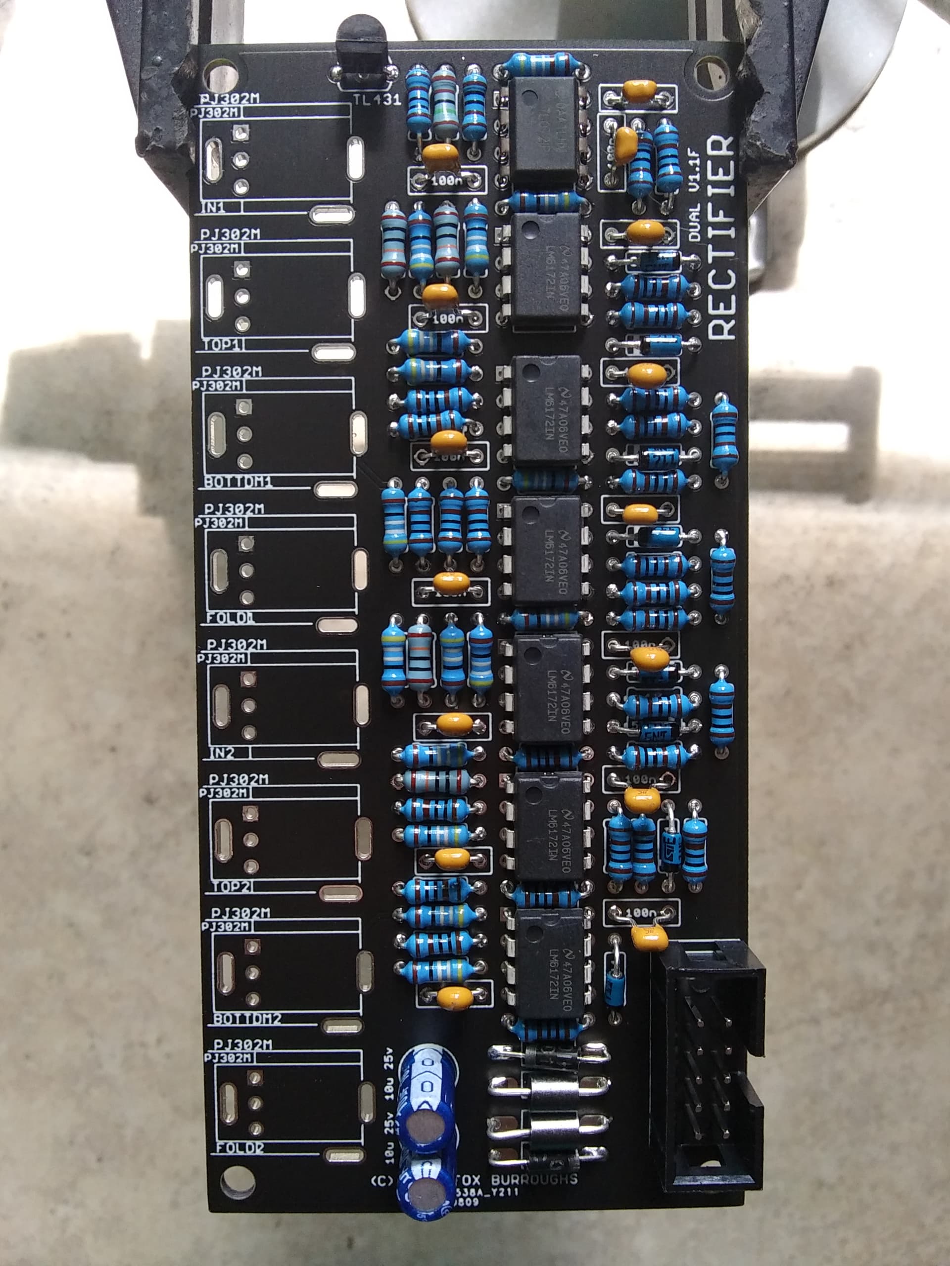
Step 11.
Place all eight of your PJ302M jacks in place and carefully install the faceplate before soldering. The faceplate is reversible so you may choose whichever side suits you.
Finger-tighten a nut onto each jack and make sure they are lined up straight. Once they are, you may solder them in place.
At this point, it is a good idea to use some isopropyl alcohol and a tooth brush to clean the bottom of your board and remove any crusty solder flux. Once it is clean, take a good long look for any solder blobs or cold joints. Fix as necessary and test. Enjoy!
#4 — saiteron · 2021-09-09
interested in a few PCB/panel sets of each!
#6 — Midcitysteve · 2021-09-10
Can I get 2X A+B-C and 1X rectifier, all pcb’s please