LZX Show & Tell, lzxpcb-fpga12 / ESG3 review
Category: Uncategorized · Tags: — · Posts: 33
#1 — creatorlars · 2022-01-19
We thought some of you may enjoy seeing some behind-the-scenes action, so I’m going to try to post more on that topic.
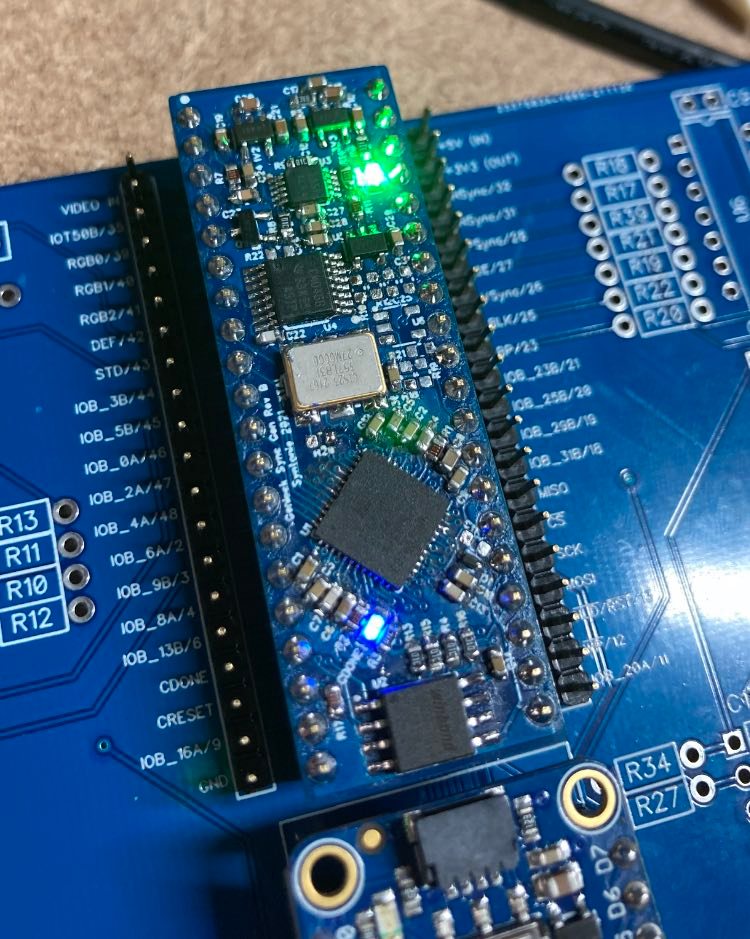
Today we reviewed a new PCB that came in last week, lzxpcb-fpga12hp-RevA The workshop team built 5 of these up yesterday. This is the third “outer layer” variant for Gen3, and is a general purpose power entry and FPGA subsystem PCBA. The first two modules that will use this assembly include ESG3 and DSG3.
This board is similar to our existing power entry + sync separator board (p/n lzxpcb-sync12), but adds an HD/SD Clock Generator and a small Lattice ICE5 series FPGA. In ESG3, this FPGA’s firmware is responsible for everything related to generating the timing of the video encoder’s outputs.
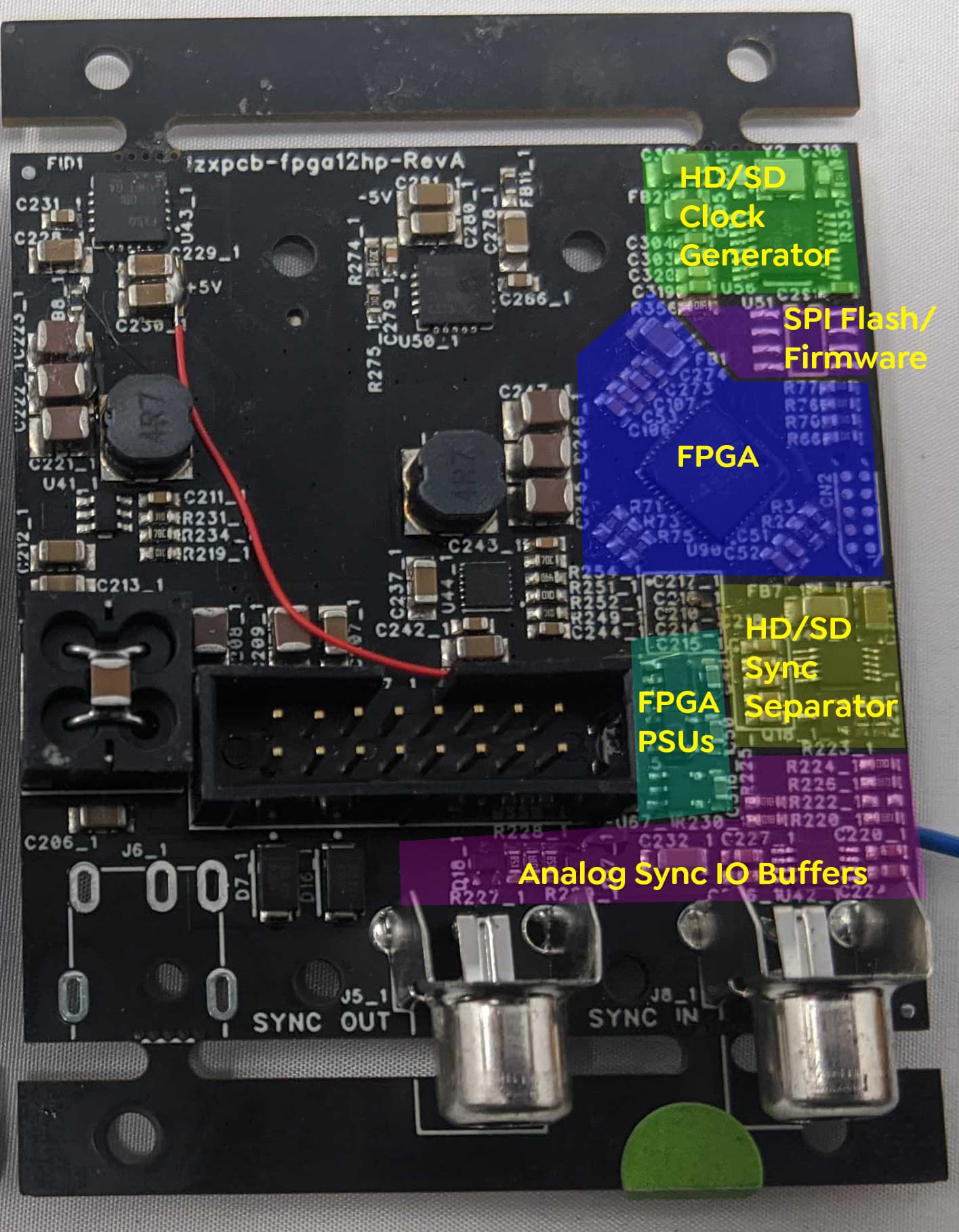
Another feature we like on this board is the Tag-Connect programmer footprint! We finally decided to give these spring-loaded pin cables a go since our footprint demands were so small on this board.
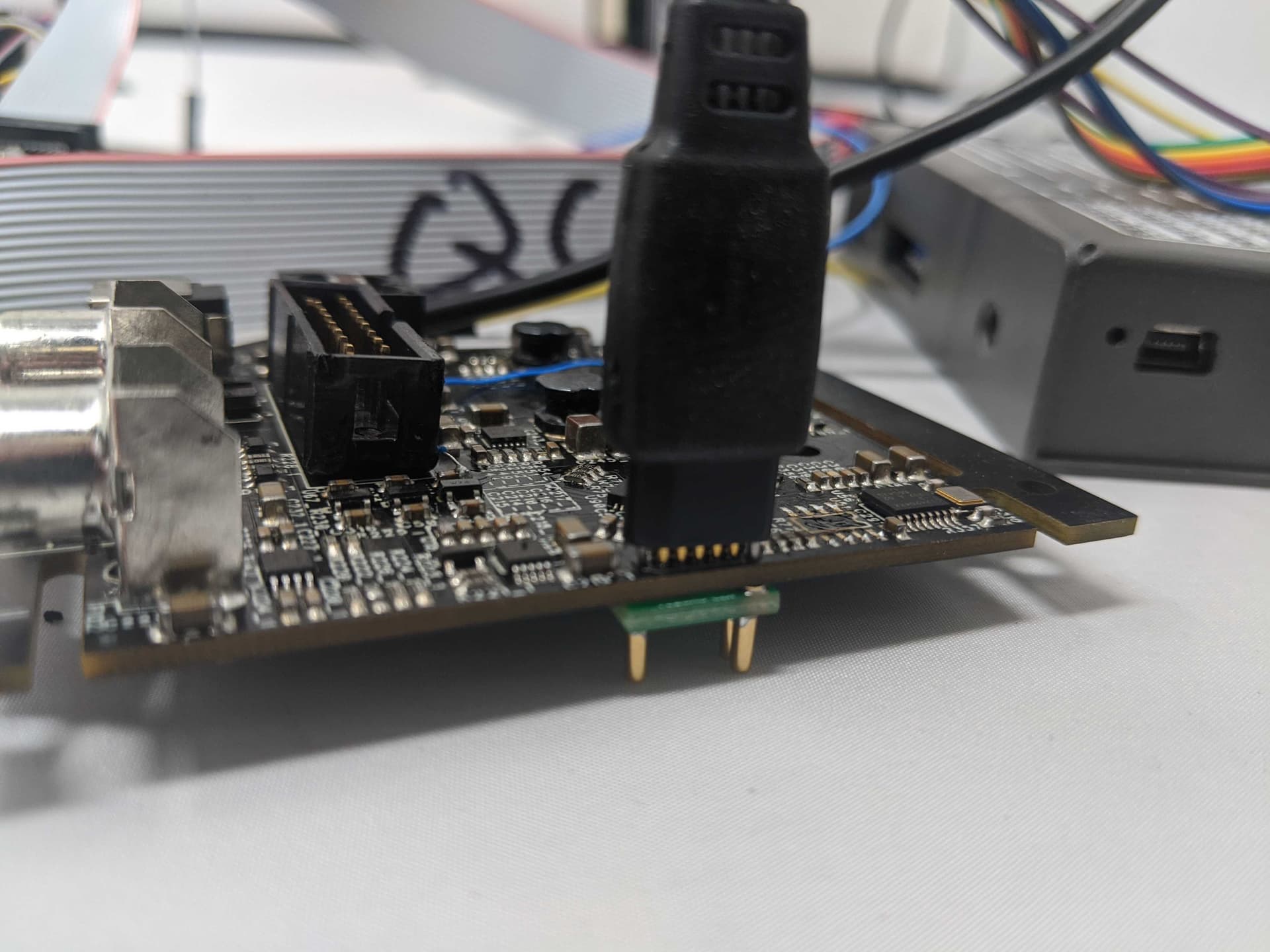
At the end of the day we’ve got our test articles all powering up, with firmware uploading successfully! With this confirmed, tomorrow we move on to testing our other new review board this week: lzxpcb-esg3-core. If that one looks good, we’ll be one big step closer to greenlighting this project.
Here’s the earlier esg3 prototype, showing our first approach (which had the FPGA on the core assembly instead of the upper power entry board.)
I hope you enjoyed seeing some process photos, let us know if you want to see more of this kind of thing, and if so, what parts of the process you like seeing most.
#2 — joem · 2022-01-19
I definitely like seeing this kind of thing and hearing about design choices.
If you don’t mind me asking, how come you moved that stuff to the power/sync board? Needed the space on the other board? Or some other reason(s)?
#3 — creatorlars · 2022-01-19
joem wrote:
If you don’t mind me asking, how come you moved that stuff to the power/sync board? Needed the space on the other board? Or some other reason(s)?
This is a new shared assembly, which means we can maintain the same board for all projects that need HD/SD sync generator and small FPGA capabilities. The big gain is to only be putting an FPGA subsystem on a single board, but use that board in multiple products.
- power only (lzxpcb-psu8)
- power + sync input (lzxpcb-sync12)
- (and this is) power + sync generator w/genlock (lzxpcb-fpga12)
Subassemblies like this make everything more testable and easier to maintain. For exampe, if at some point in the future we need to use a different FPGA part other than the ICE5, we could just revise this PCB while still maintaining pinout compatibility with all the other assemblies that use it.
There are some other benefits too. For example, the esg3-core board is now a more modular analogue output encoder assembly. If in the future we wanted to have two encoders on a single device, we could potentially use two of these assemblies (without having to have redundant FPGAs.)
We had a similar assembly to this in the Visionary series, with the logic modules! The Dual Flip Flops, Logic, and Counter modules all shared a common power + CPLD assembly.
#4 — phosphenes · 2022-01-19
Catchy name!

Always a pleasure getting a look behind the scenes and nerd out over some PCB design
#5 — VanTa · 2022-01-19
Amazing!
Really interesting to understand the decision making behind and to see in the detail the boards. Thanks for the insights!
#6 — nerdware · 2022-01-19
I’m always going to enjoy pics like these. Thanks.
#7 — creatorlars · 2022-01-20
Here are some more photos from today.
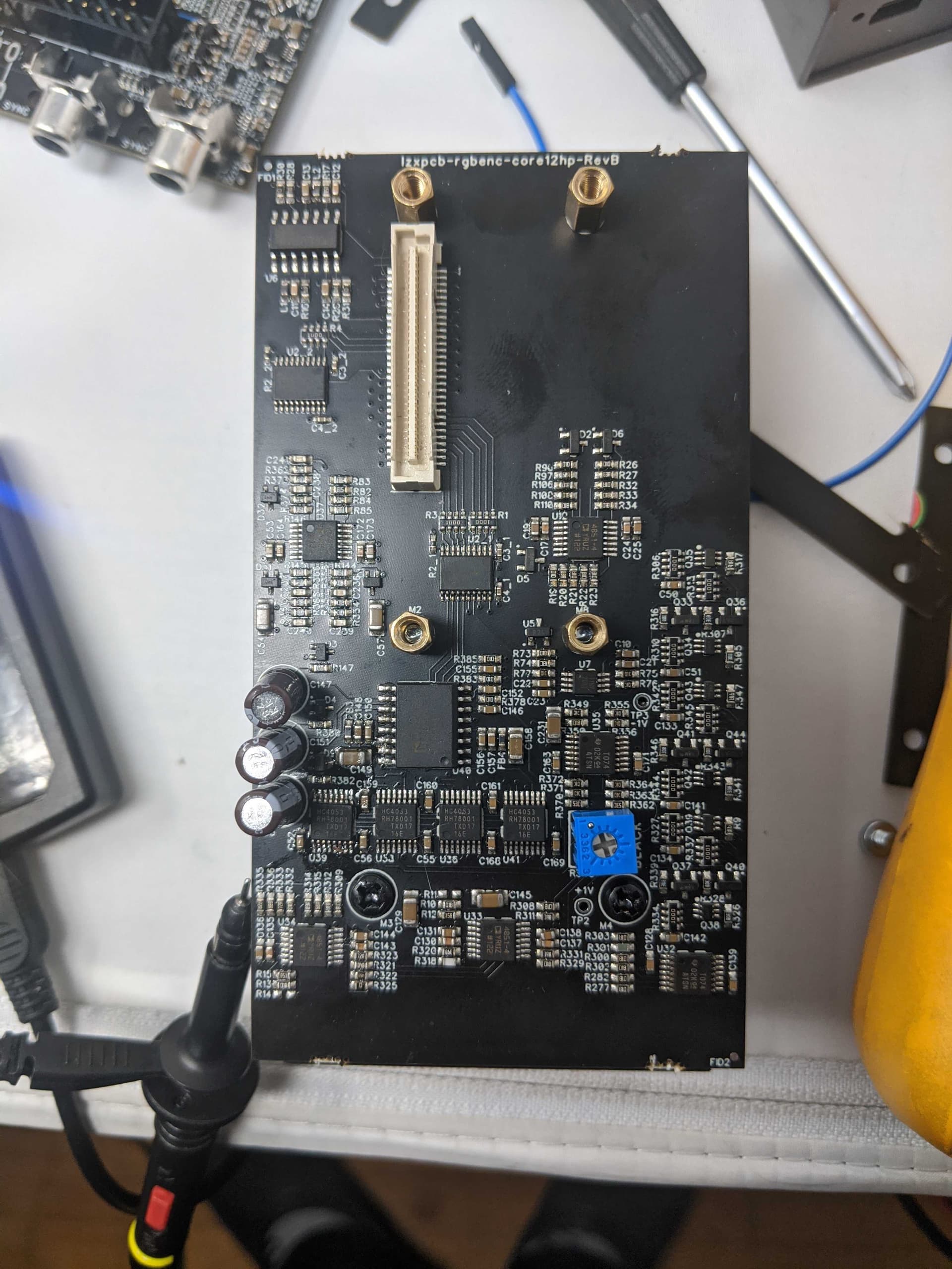
The ESG3 core PCBA. This board contains 5V/3.3V level shifters, discrete RGB blanking, Component & Composite Video Encoders, an RGB to YUV conversion matrix, and sync combination buffers.
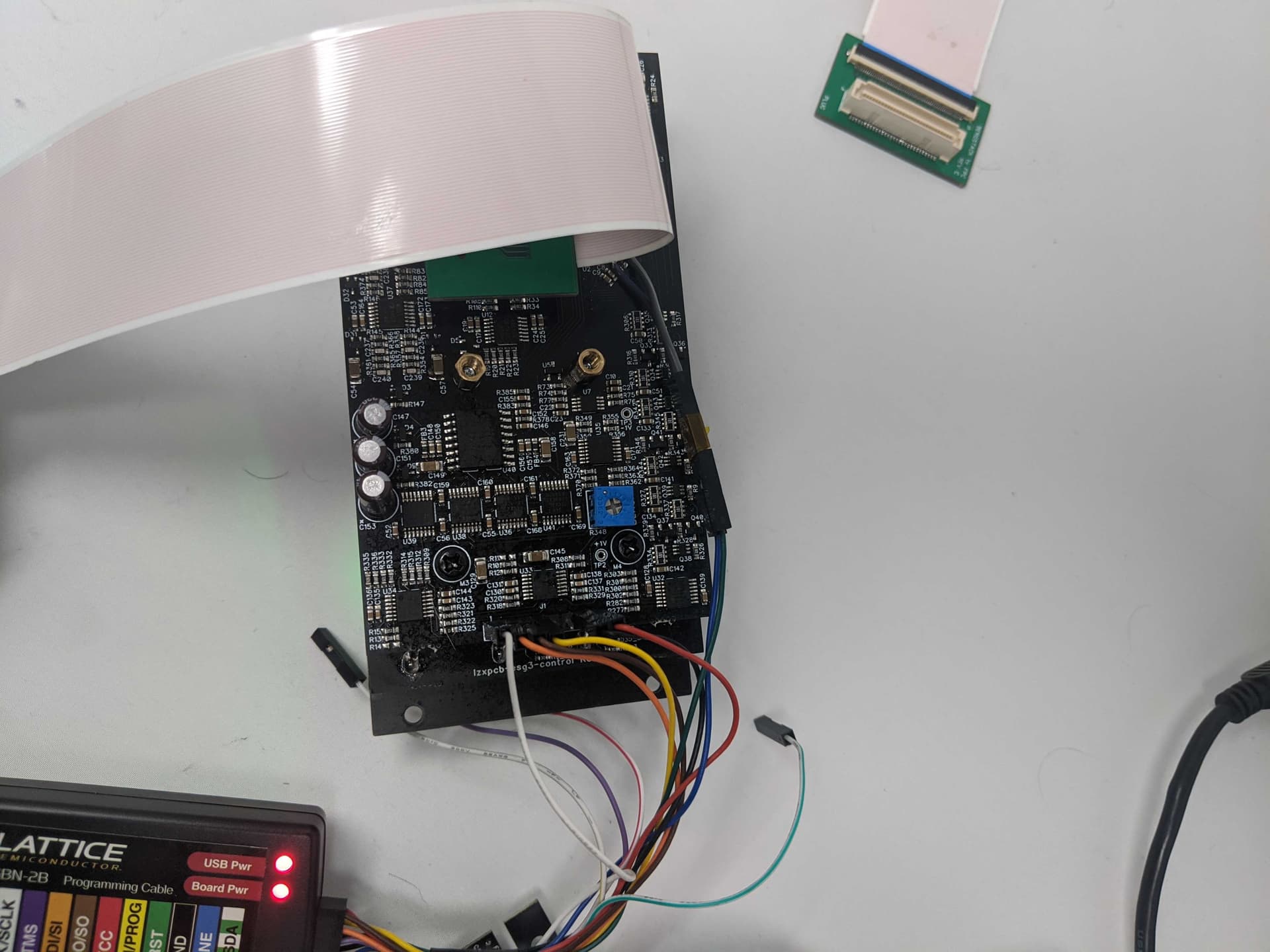
The whole ESG3 assembly. The control board (bottom left) contains the RGB procamp, which uses VCAs and exponential converters. It also contains input buffers, multiplexed RGB inverters and control logic, and some output buffers.
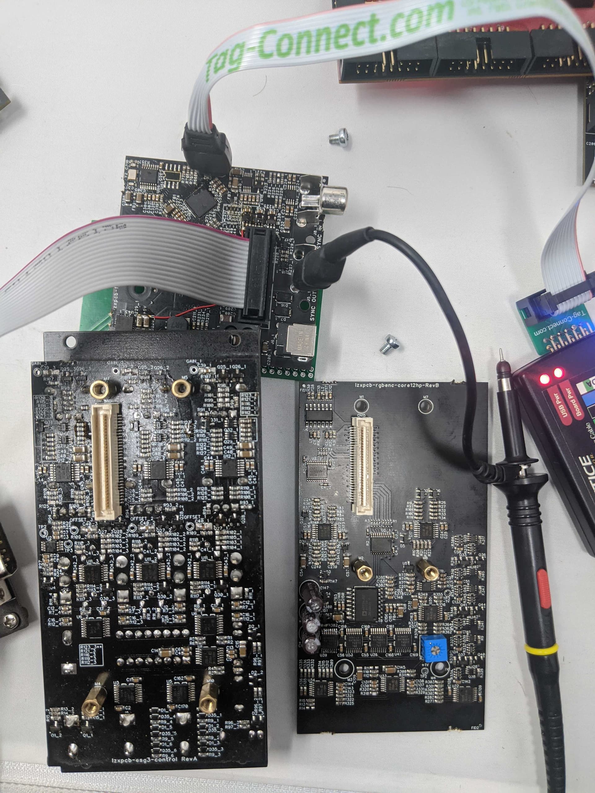
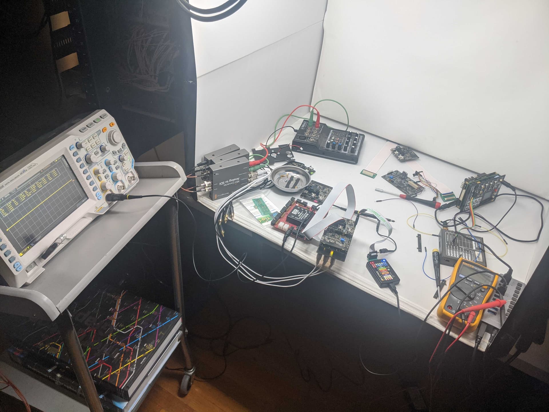
Testing in the light tent is proving highly productive. It makes a nice staging box for the current device under test and any adapters, programmers, or test leads.
#8 — vhsdestroyer · 2022-01-20
Love seeing this stuff, thanks for posting these updates!
#9 — jwsmithwick1 · 2022-01-20
Thank you for sharing those photos and letting us be flies on the wall at LZX as you bring these designs to fruition. Personally, I have a new found appreciation for the complexity of the gen3 circuits, at least from the density of the components. I have no intention of disassembling my modules, so I would have never really had the opportunity to see what was going on under the hood. Cheers!
#10 — creatorlars · 2022-01-21
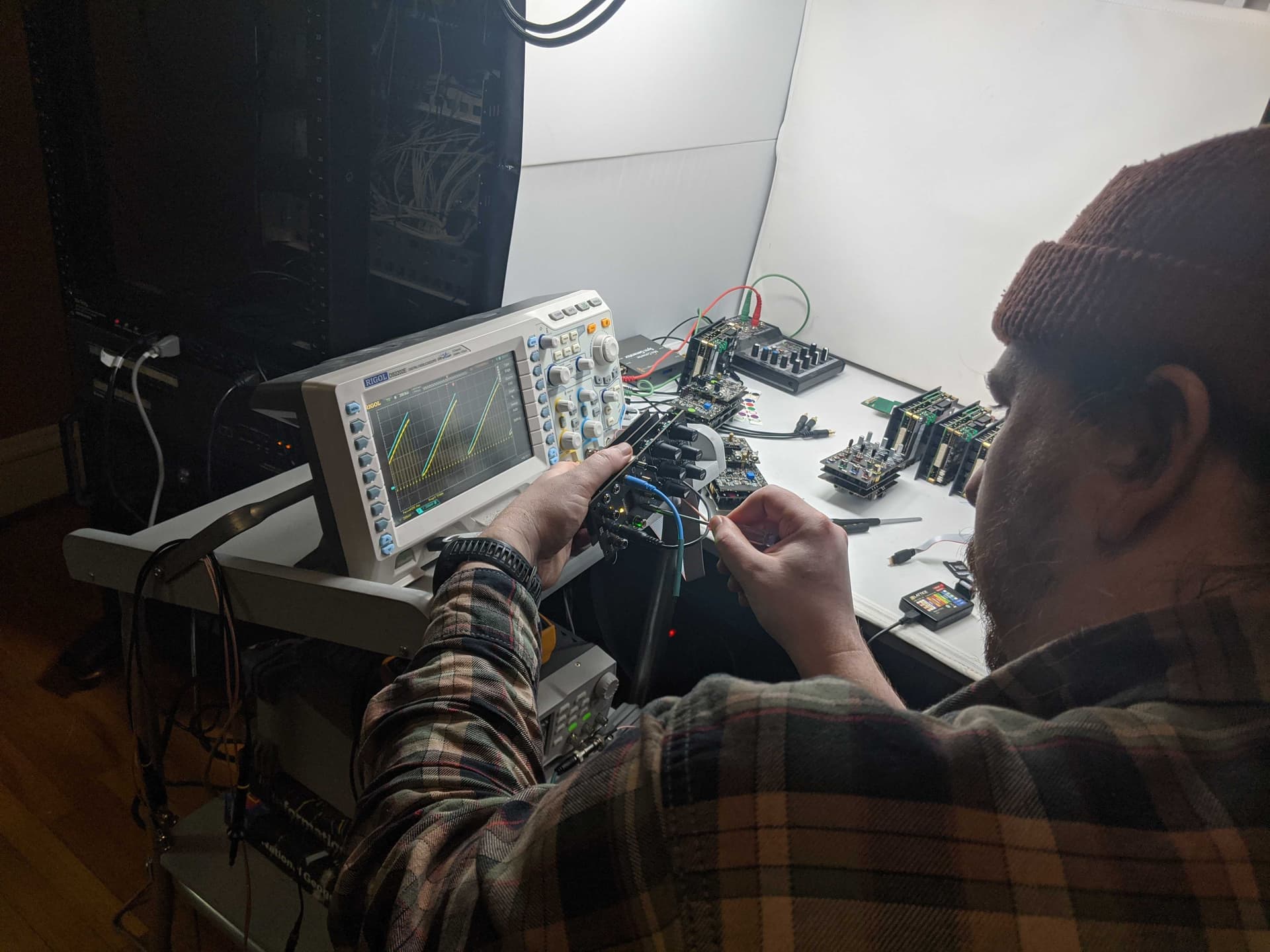
This is a very simple example, but here’s a look at a step in what’s involved with hardware design verification & testing.
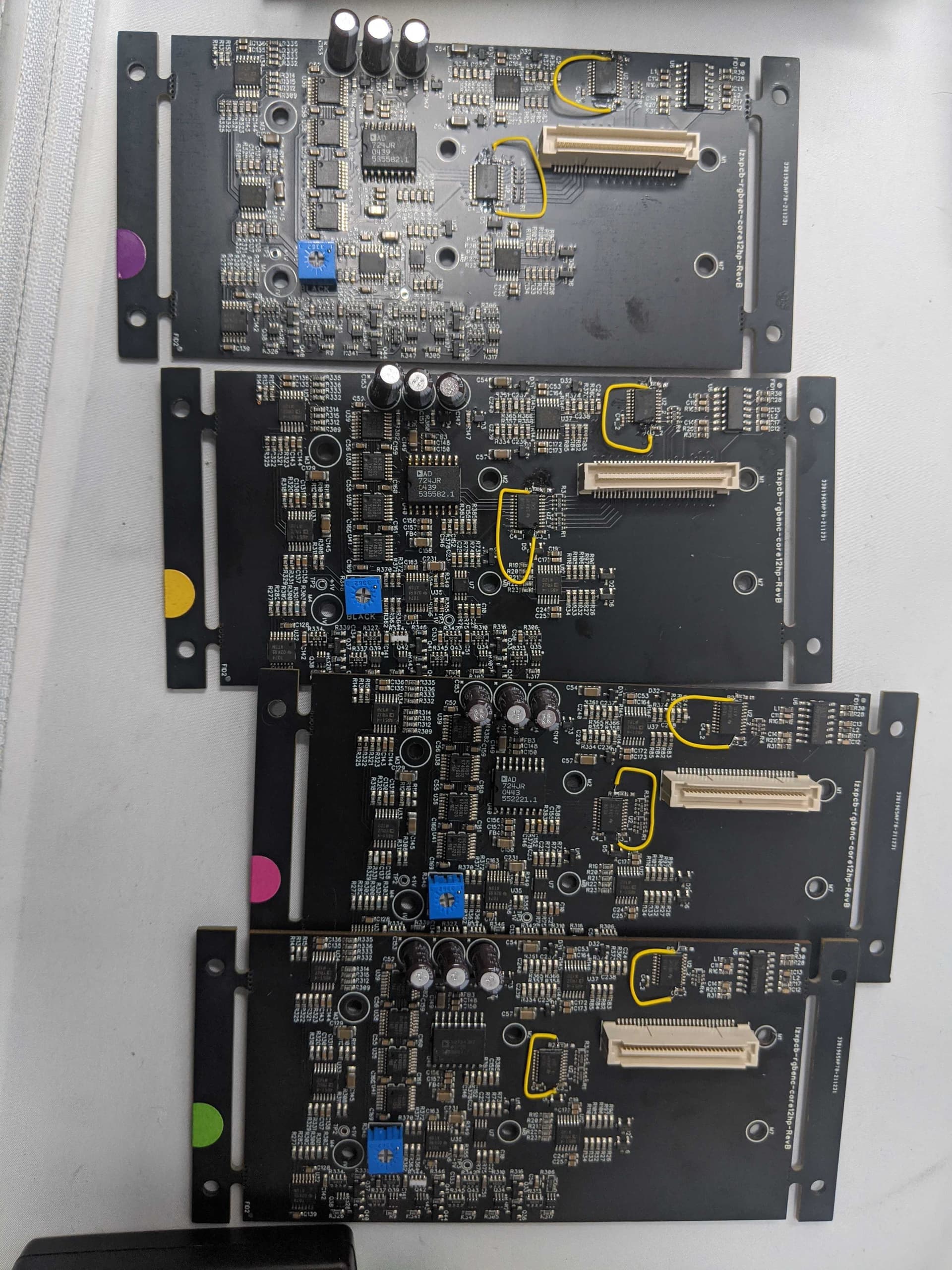
After initially powering up an assembly, an important next step is to get 3-5 samples built that are also passing the same tests. We scribble a lot of notes as we go, and use color coded stickers to identify individual boards.
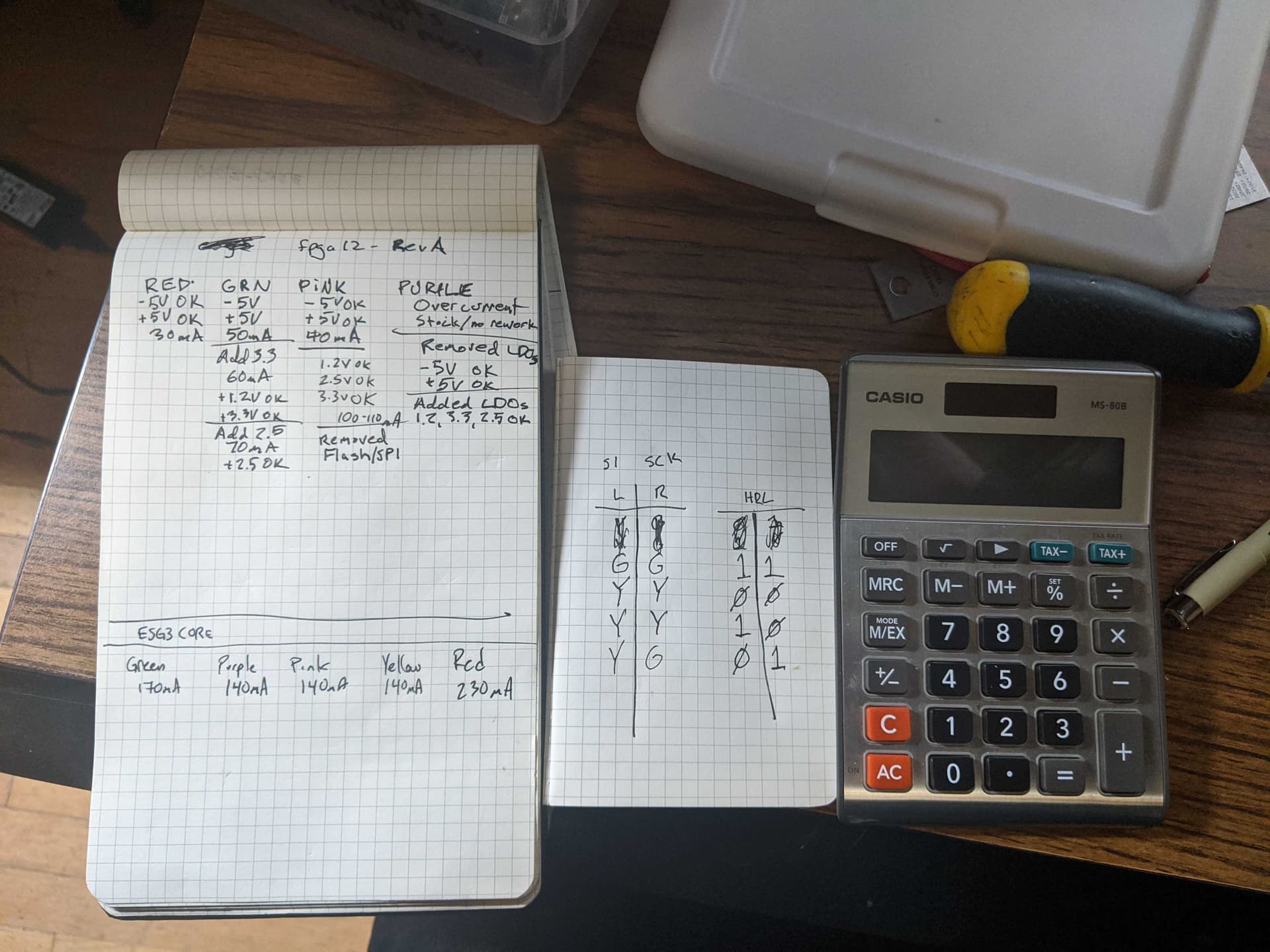
After making sure 5x ESG3 articles (assembled from the three sub-assembly boards) were fully powering up to the same current draws, we can write some simple firmware to verify the FPGA.
Here’s a VHDL snippet showing what some very simple code looks like to increment a counter and use the most significant bits of that register to make the frontpanel LEDs blink.
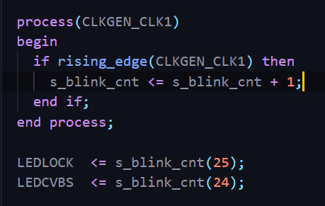
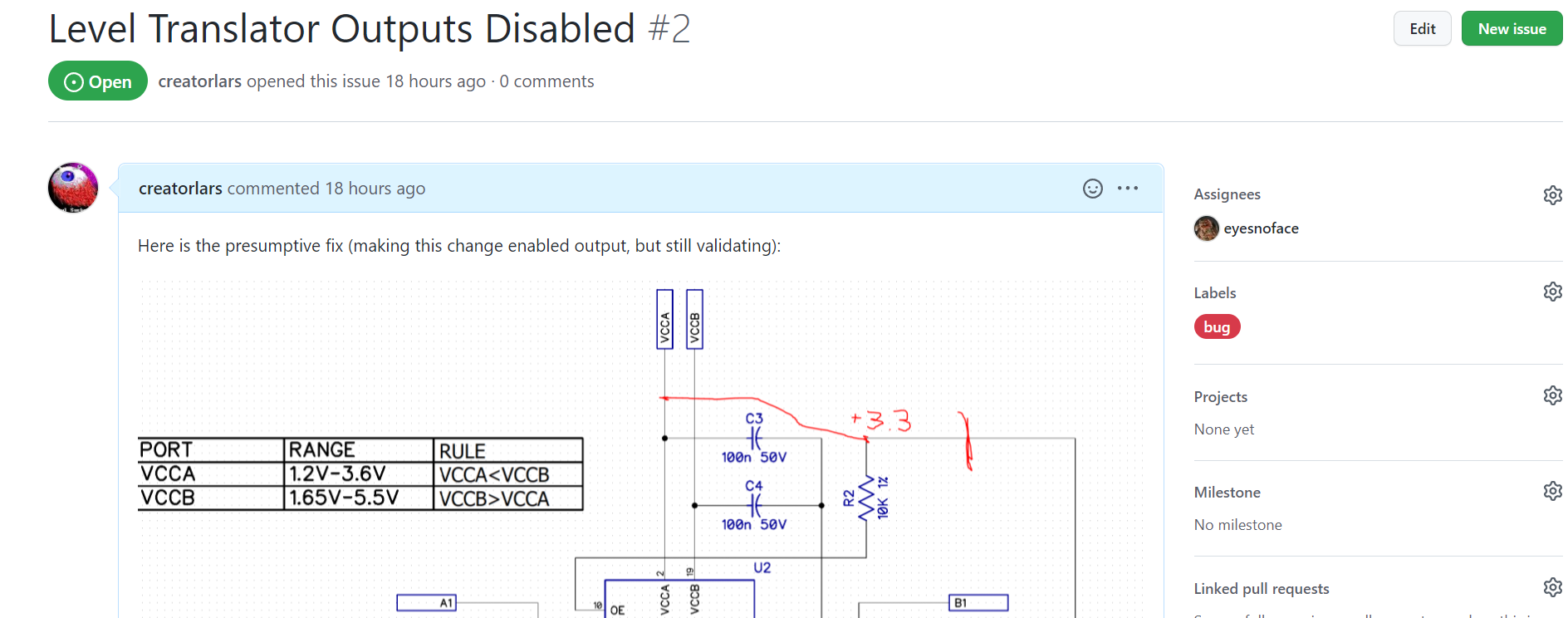
We compiled and programmed the firmware binary onto the FPGA, but nothing happened. It’s very rare that everything works on the first try, though. So the next step was to do some investigation. We traced the LED connections in our schematic through the assemblies, trying to come up with theories about why the LEDs were not blinking yet.
Naturally, the first places to look are places this circuit has changed since it’s last version. That led us to the new level translators on the new version of the core PCBA. Oops! We forgot to add a pullup on this part, which meant the level translator outputs were disabled. No wonder the LEDs weren’t blinking.
Usually we’d dig around for a few more theories before the hardware measurements start, but in this case we were pretty sure this was our issue. We made a quick fix to one board: problem resolved!

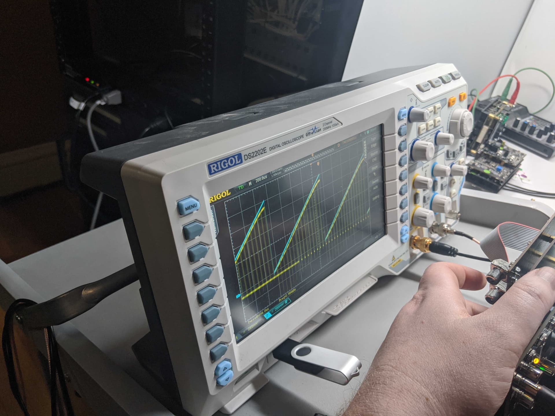
Since we got that far, we checked for video output, which was present:
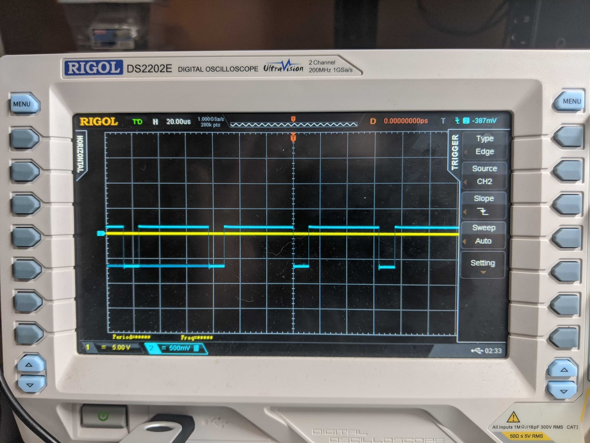
(Homework: Can anyone determine the video format from this scope shot?)
This is an important milestone, since we now know that there is communication across all three PCBs functioning as expected, that our clock generator is running, and that video sync is being generated.
Before getting carried away though, we need to make sure to accurately log our issue and the rework performed in GitHub. This way we’ll have all the notes we’ll need to revise the PCB layout and schematic later, after the review has been completed.
We also make sure we’ve fixed the issue on our other four test assemblies, so fixes can be confirmed multiple times over before we commit to them.
#11 — rempesm · 2022-01-22
This is all very fascinating to see, thank you for letting us in on the behind the scenes development!
#12 — creatorlars · 2022-01-22
A few end of the week photos. We finished validating the new hardware today. We need to write up some calibration instructions for the workshop team going into next week and run a few more tests, then we’ll be able to sign off on production hardware.
a quartet of video encoders
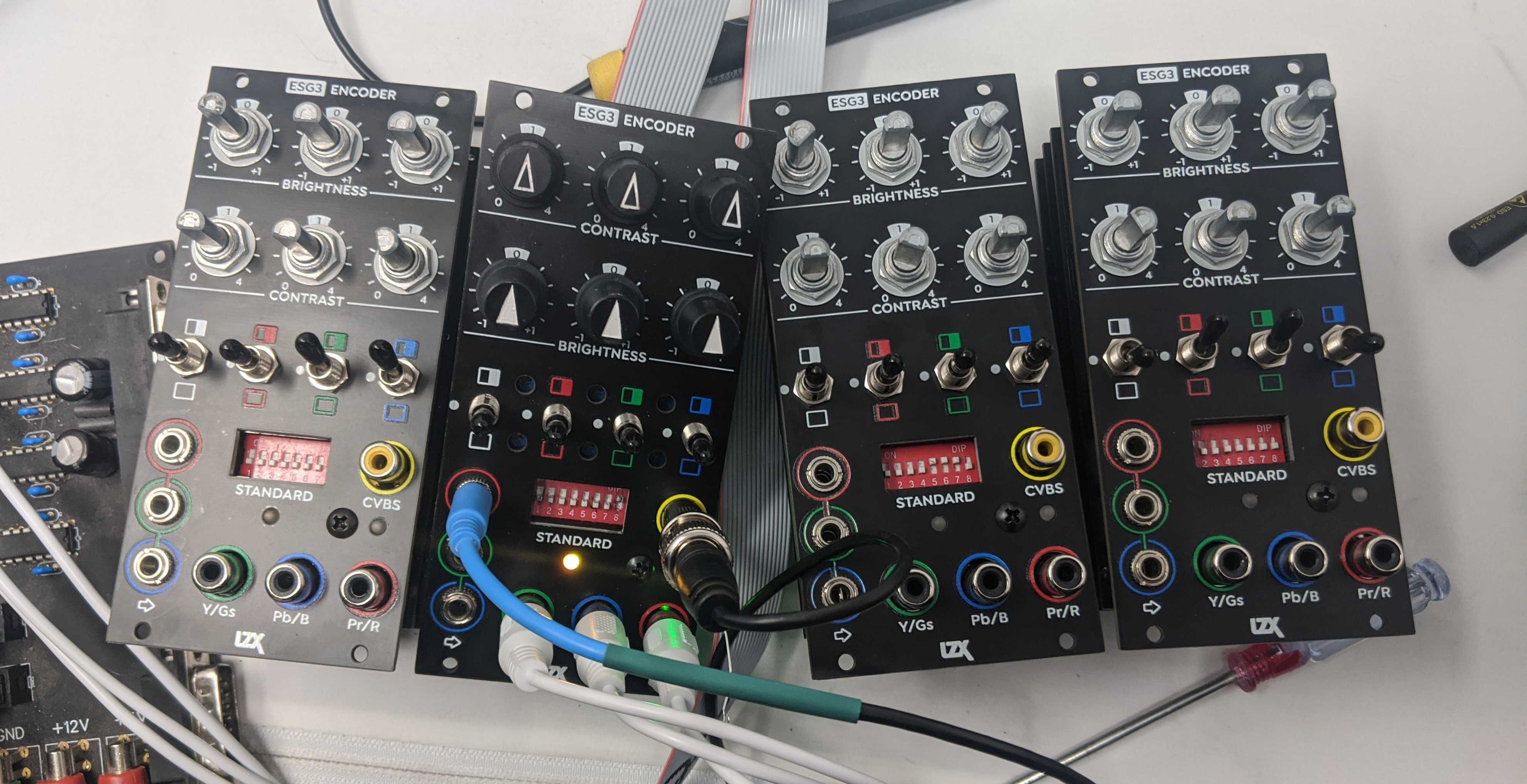
@eyesnoface calibrating RGB gain/brightness using test ramps
#13 — syntonie · 2022-01-22
Thanks for sharing details on the hardware/software, being working on my own sync gen, it is super interesting to see!
Also great to see some love for Lattice FPGAs, I started my project using a Xilinx Coolrunner CPLD (as it is used on your older generations of modules iirc), then they are a little small in terms of macrocells/LUTs, so Eric Schlappi convinced me to look into the iCE40. It asks for a few more extra support components (SPI Flash and 1.8V regulator in addition to the 3.3V one), but the UP5K part comes in QFN package (which can be soldered by hand), has about 5K LUTs and is supported by the iCEstorm open source toolchain.
I was tempted using LMH1982 for the clock generator at first, though they’re quite expensive, so went for the PLL+VCXO as shown on Cadet I, looks like that what you’re using here too right? Also, we can see that the flash chip isn’t populated, I presume you’re writing the bitstream directly to the FPGA SRAM?
Hope I’m not annoying with my questions/sharing about my stuff, I’m pretty new to FPGAs and been learning through resources online until now, then this is pretty exciting to see a video sync generator implementation to me!
Here is the board I did, in DIP40 format to be used in DIY projects, with regulators at the top, then sync extractor, PLL+VCXO, iCE40 and finally flash (pardon the poor hand soldering, those tightly spaced 0603 were not super easy to fit). It is greatly inspired by iCEbreaker/UpDuino devboards.
creatorlars wrote:
From the time base, we can see that the pulses occurs every ~64us, so would be either 480i or 576i format. Then from the length of the pulses (~10us) we can guess that this is a blanking signal (and the continuous line on the left would be vertical blanking).
#14 — 337is · 2022-01-22
Might be the wrong thread to ask, but with the variants involving sync & blackburst, will any of the planned gen3 modules have a sync pass through from front panel to back panel that doesn’t involve burning a camera input? Still eager for a solution to unite front of house and back of house sync throughout multiple cases without needing to DIY, leave a blank space in the rack, or waste a video input.
#15 — creatorlars · 2022-01-22
Might be the wrong thread to ask, but with the variants involving sync & blackburst, will any of the planned gen3 modules have a sync pass through from front panel to back panel that doesn’t involve burning a camera input?
Short answer: Yes. TBC2 has front and rear sync input and output separate from any video IO. That’s the Gen3 module with this feature.
Longer answer: A few utility modules should be added after the launch of the first set (TBC2, Chromagnon, ESG3, DSG3, FKG3, SMX3, DWO3). We’re hesitant to rush into any of them because we want to poll the community after you’ve all spent time patching these. But a general purpose sync/video distribution amplifier, with front and rear IO, seems like a must.
#16 — creatorlars · 2022-01-22
Also great to see some love for Lattice FPGAs
Yes, it has been pretty pain free to work with so far! The form factor is perfect for this use case. Not as fast as the fabric in the Xilinx parts we’ve been using, but so many more resources, smaller package sizes, than something like the CoolRunner CPLDs we used in Fortress/Visual Cortex. We needed a part where we could port our sync gen/timing HDL modules from TBC2/Chromagnon directly and maintain a common codebase, so the CPLD wasn’t going to cut it for this project (but the Zynq much too large/expensive to put on a typical module.) So LP5 has become our “small system” and Zynq our “big system.” The new Zynq board we’ve been working on for Chromagnon is modular too. So an “even bigger system” (like for a future vector-to-raster device) could be realized with multiples of the Zynq board. One of the mistakes with Orion series we made was experimenting with too many embedded system approaches! So I hope we can keep it to just LP5 and Zynq, and some small MCUs, for projects in the foreseeable future.
Also, we can see that the flash chip isn’t populated, I presume you’re writing the bitstream directly to the FPGA SRAM?
Yes, for development we’ve just been writing directly to the CRAM with the Lattice programmer tools. For production the firmware will be written to the Flash, and the part will program from that.
I was tempted using LMH1982 for the clock generator at first, though they’re quite expensive, so went for the PLL+VCXO as shown on Cadet I, looks like that what you’re using here too right? Also, we can see that the flash chip isn’t populated, I presume you’re writing the bitstream directly to the FPGA SRAM?
We’re using the LMH1980 for sync separator and the Cypress 24204 for clock generator. The Cypress part has an integrated 27MHz VCXO but also generates the two HD clocks (74.25MHz and 74.25/1.001MHz). Inside the FPGA we are using the internal PLL to create a 108MHz clock that drives the 3.58MHz and 4.43MHz NTSC/PAL subcarrier generators (FSC clock for AD724 encoder.)
You can read more about the Cypress part here:
micro-semiconductor.comhttps://www.micro-semiconductor.com/datasheet/6e-CY24204ZXC-3.pdfhttps://www.micro-semiconductor.com/datasheet/6e-CY24204ZXC-3.pdf229.62 KB
Link: 6e-CY24204ZXC-3.pdf
syntonie wrote:
From the time base, we can see that the pulses occurs every ~64us, so would be either 480i or 576i format. Then from the length of the pulses (~10us) we can guess that this is a blanking signal (and the continuous line on the left would be vertical blanking).
Correct! Yes, this is NTSC. You’re actually just seeing the video output itself here, but without any image content.
#17 — syntonie · 2022-01-22
creatorlars wrote:
The form factor is perfect for this use case. Not as fast as the fabric in the Xilinx parts we’ve been using, but so many more resources, smaller package sizes, than something like the CoolRunner CPLDs we used in Fortress/Visual Cortex. We needed a part where we could port our sync gen/timing HDL modules from TBC2/Chromagnon directly and maintain a common codebase, so the CPLD wasn’t going to cut it for this project (but the Zynq much too large/expensive to put on a typical module.) So LP5 has become our “small system” and Zynq our “big system.”
Right, the iCE serie seems a bit limited to be used for video processing, even more when talking about HD video, though perfect for sync/signal generation purposes. Lattice ECP5 sounds more like a good candidate for this from what Schlappi told me, though it would probably asks for a µC to go with it, so the Zynq serie makes a lot more sense in that case!
creatorlars wrote:
We’re using the LMH1980 for sync separator and the Cypress 24204 for clock generator. The Cypress part has an integrated 27MHz VCXO but also generates the two HD clocks (74.25MHz and 74.25/1.001MHz). Inside the FPGA we are using the internal PLL to create a 108MHz clock that drives the 3.58MHz and 4.43MHz NTSC/PAL subcarrier generators (FSC clock for AD724 encoder.)
That clock generator part is neat! Most of dedicated ICs I found for this were obsolete, and LMH1982 was bit out of the scope in term of price range, so went for the 4046 + 27MHz VCXO route, even though it has some drawbacks such as jitter and resting frequency. Also, I was able to generate a 74.25MHz clock out of the 27MHz VCXO on my board, though 74.25MHz/1.001 couldn’t be achieved with the internal FPGA PLL, so doesn’t allow for 29.97Hz/59.94Hz timings. That’s nice that you can also generate chroma subcarriers from the FPGA, save some board space and cost by not using dedicated crystal oscillators.
Thanks again for the insight on this!
#18 — creatorlars · 2022-01-22
syntonie wrote:
That clock generator part is neat! Most of dedicated ICs I found for this were obsolete, and LMH1982 was bit out of the scope in term of price range, so went for the 4046 + 27MHz VCXO route, even though it has some drawbacks such as jitter and resting frequency. Also, I was able to generate a 74.25MHz clock out of the 27MHz VCXO on my board, though 74.25MHz/1.001 couldn’t be achieved with the internal FPGA PLL, so doesn’t allow for 29.97Hz/59.94Hz timings.
Yeah, the Cypress part is nice. It’s no more expensive than a standalone VCXO+4046 circuit like you’re doing now – we have the VCXO phase comparator inside the RTL on the FPGA. I think we’re going to see more of a low cost market for this particular era of set top box / video encoding IC over the next few years. A lot of the parts that were designed for mass produced SD/HD equipment up to 1080p30 (like this part) are now being deprecated for new devices that use 4K compatible or 1080p60 parts – so there will be excess stock of NOS parts, etc.
Also; another point of putting the FPGA on a subassembly (like we both did!) is that if we need to change the clock generator approach at some point, there are many ways to do that. I would not like having the 24204 on multiple product-specific boards. If we had used a shared assembly with Cadet and Visual Cortex, for example, it would have been easier to update and maintain those designs.
That’s nice that you can also generate chroma subcarriers from the FPGA, save some board space and cost by not using dedicated crystal oscillators.
Yes, and there are some technical advantages to having a subcarrier that is synchronous (PAL “super-frame”) with the sync generator source – it eliminates dot crawl and can result in cleaner analog to digital conversion.
We’ll definitely be working on some DCO engine implementations for this ICE5, and various direct logic functions. I’m not sure what else. It would be interesting to simulate a minimal microcontroller on it, capable of using the SPI or I2C blocks, along with an RTL video function.
#19 — dryodryo · 2022-01-23
I don’t understand the alphabet soup, but it sure is cool to see the progress.
Rock on
#20 — VanTa · 2022-01-23
This is the kind of post that I know I’ll come back in one year or so and say: aha! All the info I need is here!
Loving it

#21 — 337is · 2022-01-23
Thanks for the answer and explanation Lars. I look forward to the community polling and possible utility modules to come. I’d love a TBC2 in every case but that’d be a costly move. Fun, but too rich for my blood.
#22 — creatorlars · 2022-01-23
Thanks for the answer and explanation Lars. I look forward to the community polling and possible utility modules to come. I’d love a TBC2 in every case but that’d be a costly move. Fun, but too rich for my blood.
Oh that’s certainly not the expectation for large, multi-case systems! I imagine a 12HP sync distributor module is a good idea, and that we try to fit any legacy conversion/adapter needs into that one module. It would be the module you put in any “expander case” that does not otherwise include something like TBC2. The size of folks’ cases and what modules they are distributing sync to are all factors that come into play in the design of this, and we need to poll for user needs in this area before arriving at a final answer.
TBC2 makes a good “crosspoint” between systems mainly due to the internal dual channel upscaler/downscaler. (Have we mentioned yet, that you can upscale and downscale between any of the 15 SD/HD video formats, with different formats on the input channels?) So, for example, if you have a case with an SD system/device interfacing to a case running as an HD system/device, the TBC2 is exactly where you want the sync to come in and be distributed from.
#23 — jwsmithwick1 · 2022-01-23
@creatorlars , I agree with @337is . It would be really useful to have a utilities module that provided the HD versions of the Visual Cortex sync generator outputs as well as the raw HD H and V ramps. It would be great to sync oscillators to those signals as well as process them with the modules I enjoy using. In addition, the module could have front and rear sync RCA. There might be even more space for other features, like a multiple. I feel like that would be a good way to integrate the Gen3 modules with compatible video modules. It’s great to hear that something like this module is somewhere on the horizon.
Maybe call it the LSD3, Legacy Sync Distributor

#24 — creatorlars · 2022-01-23
jwsmithwick1 wrote:
@creatorlars> , I agree with > @337is> . It would be really useful to have a utilities module that provided the HD versions of the Visual Cortex sync generator outputs as well as the raw HD H and V ramps. It would be great to sync oscillators to those signals as well as process them with the modules I enjoy using. In addition, the module could have front and rear sync RCA. There might be even more space for other features, like a multiple. I feel like that would be a good way to integrate the Gen3 modules with compatible video modules. It’s great to hear that something like this module is somewhere on the horizon.
Yes – effectively this is a variation of DSG3 and could be implemented with a new control board for that module. Instead of two shape generators, you would have a bunch of fixed output ramps, and HSYNC/VSYNC could be among them, as well as a front panel sync input. So a bit less powerful than DSG3 in terms of combinatorial capabilities (no input proc capabilities), but it would support a similar workflow to Visual Cortex – and provide a lot more patchable source connections. A “Gen3 Frontend” as ESG3 is the “Gen3 Backend”?
#25 — creatorlars · 2022-01-24
@337is Or maybe you were thinking something simpler? A passive RCA pass-thru connector panel is easily something we can offer if that’s what’s needed.
#26 — 337is · 2022-01-25
This simple pass through would be a boon but am curious about the possibilities you mentioned too. Some sort of super utility module could be useful. I wasn’t joking when I said I could have a Bridge and Passage multiple times in every row. A Bridge with RCA mults front and back would do work. Offsets/attenuators combined with that would be even dreamier. This sort of signal traffic director for any signal between cases and between front and back of house. A synced mult is endlessly useful to me. Luma to 6 Bridges finds applications in my system. Pack those 12 HPs six ways to Sunday to help me setup meaningful trunk lines in each case, row, whatever. Rambling I know, but even though I despise HDMI, it gets one thing right by carrying ALL THE SIGNALS. Anything that can help centralize and move our various signals from where they are to where they need to be would be helpful.
#27 — creatorlars · 2022-01-25
337is wrote:
Some sort of super utility module could be useful. I wasn’t joking when I said I could have a Bridge and Passage multiple times in every row.
Pack those 12 HPs six ways to Sunday
I think there’s what I have in my head as the “voltage lab” module, like this, or it’s a type of module, that embraces high density of raw patchable function blocks. An extension of Bridge/Arch really! Into the more functionally dense 12HP gen3 stack format. Another very Gen3 way to do things is to do a multi-mode function block or array of some kind (for example, a logic function with 8 logic modes on a rotary switch.) It will be fun to workshop some ideas like this. That conversation can begin with what people already like about Bridge and Arch and how we could improve on those.
#28 — jwsmithwick1 · 2022-01-25
I feel having an abundance of core source connections will allow of the integration of modules that I already own and love, like the Synontie wave shaper, The Prismatic Ray, etc. If I were to use the DSG3 just to make raw ramps, I feel like would be under using that module. I’m thinking of module that combines an HD sync generator with a few core video ramps and RCA front panel sync. This could be used in tandem with a TBC2 in a multi case or 6U x 6U travel clam-shell style case so that one isn’t forced to keep all of the sync reliant modules in one of the cases.
#29 — creatorlars · 2022-01-25
We discussed this some today, and I think the idea is clicking with us – we like the idea of this as a “System Reference Module” – by definition, it’s meant to provide unmodifiable reference ramps, reference HV sync pulses, etc for distribution throughout the system. And also the perfect place to put the system’s external sync connection as well.
The main difference between how we’ve done modules like this in the past, is that the “reference module” has always been a required module (usually as the system’s sync generator), and now – due to a node based sync architecture (many modules can both receive or generate sync) we have decoupled that.
Ultimately the effect of that is that the “reference module” can fully embrace it’s own role or identity, uncomplicated from the demands of a module that every system is required to include.
This segues into the “wall of angles” concept I’ve been all about doing at some point, too – we can have a large variety of ramps of different angles and slopes, to uses as references throughout the rest of the patch.
The main thing is I want all of these combos to not only be valid, but interesting system build options, without any dead ends or redundancies:
- ESG3
- TBC2 + ESG3
- System Ref Module + ESG3
- System Ref Module + ESG3 + TBC2
And I think in context that all works in a way that I wasn’t expecting, that I quite like.
#30 — Rik_bS · 2022-01-25
- System Ref Module + Visual Cortex

A bunch of the Sync + Ramps outputs like on the VC panel’s top left and right, would be very useful.
Call it the Angles + Ramps + Sync 3
#31 — VanTa · 2022-01-25
I also agree that a bridge arch combo is really powerful. I love them together and most of the time I leave some parts of them pre patched when I start a new patch. Normaled outs from some sections into others ins, would be a nice addition for gen3 version. For example the gamma processor from arch to the fade in bridge. Or the mixer from bridge into the rectifier in arch.
What I also like a lot in those modules is the invert switches, where with a small click, your patch changes completely.
Such a module could be like the ‘maths’ of videosynth.
#32 — creatorlars · 2022-01-25
VanTa wrote:
For example the gamma processor from arch to the fade in bridge. Or the mixer from bridge into the rectifier in arch.>>>> What I also like a lot in those modules is the invert switches, where with a small click, your patch changes completely.
DSG3 is trying to really be what you’re describing (but only one possible incarnation of it.) It’s really a patchable analogue logic mix function, like Arch, where each of 4x input channels has not just a single invert switch, but several processors that can be enabled or disabled without changing the patch. (So lots of patch variety with simple IO.)
But I can see many other forms this could take, including something based more on a normalization scheme.
One thing we’re trying consider a lot is variety of approach. Some modules focusing more on “patch programming”, some modules focus more on “tuning and modulation control”, some modules focus more on “multi-modal switched signal paths/functions”, etc.
So I anticipate, with utility functions like summing, mults, mixes, voltage procs, etc we try not to encapsulate those in single modules with only one approach to them. It’s the identity of user control concept that gets encapsulated instead. So we can have something patch heavy or switch heavy or knob heavy, all of which are different workflow based approaches to common building blocks.
#33 — 337is · 2022-01-27
creatorlars wrote:
And I think in context that all works in a way that I wasn’t expecting, that I quite like.
Hooray for discoveries through discussion! Always energizing for me.