Bipolar trimmer on Cadet X multiplier rotator
Category: Unknown · Tags: — · Posts: 23
#1 — macumbista · 2022-02-24
Jason Butcher and I am working on a single-axis rotator board based on the Cadet X multiplier.
Since we want everything to be four quadrant, we are centering the 1V p-to-p ramps at 0V (so -0.5V to +0.5V). Therefore we would like the offsets in the CV inputs to be bipolar as well (trimmer between +2.5V and -2.5V).
Two questions:
- If there are four multipliers on each board (plus several op amps), can we buffer a global 2.5V using a single op amp for the entire board?
(I suspect yes, since there is no loading apart from the trimmers, but maybe they need to be isolated from each other)
- The more complicated question: can we simply op-amp invert the +2.5V from the TL431 to get -2.5V, or should we make a separate TL431 “flipped upside down” to get -2.5V to be buffered by one (or more) op amps?
Thanks!
Derek
#2 — transistorcat · 2022-02-24
Not sure exactly what the requirements for precision and stability for the 2.5V references are in the design (and the consequences of deviating from them) but the only sources of error introduced in the inverter as opposed to a non-inverting op-amp buffer are from the resistor divider (relative precision and temperature dependency).
If i’m understanding you correctly, the negative reference is only used for the trimmers, and as such already dependent on the trimmer resistance in the same way.
On the other hand, the offset signal is effectively inverted twice along the signal chain, so you should also be able to shift the trim signal down by adding a positive reference into the negative terminal of U3.2 (and possibly modifying the R21/R22 divider to increase the range of the trimmer)
#3 — macumbista · 2022-02-24
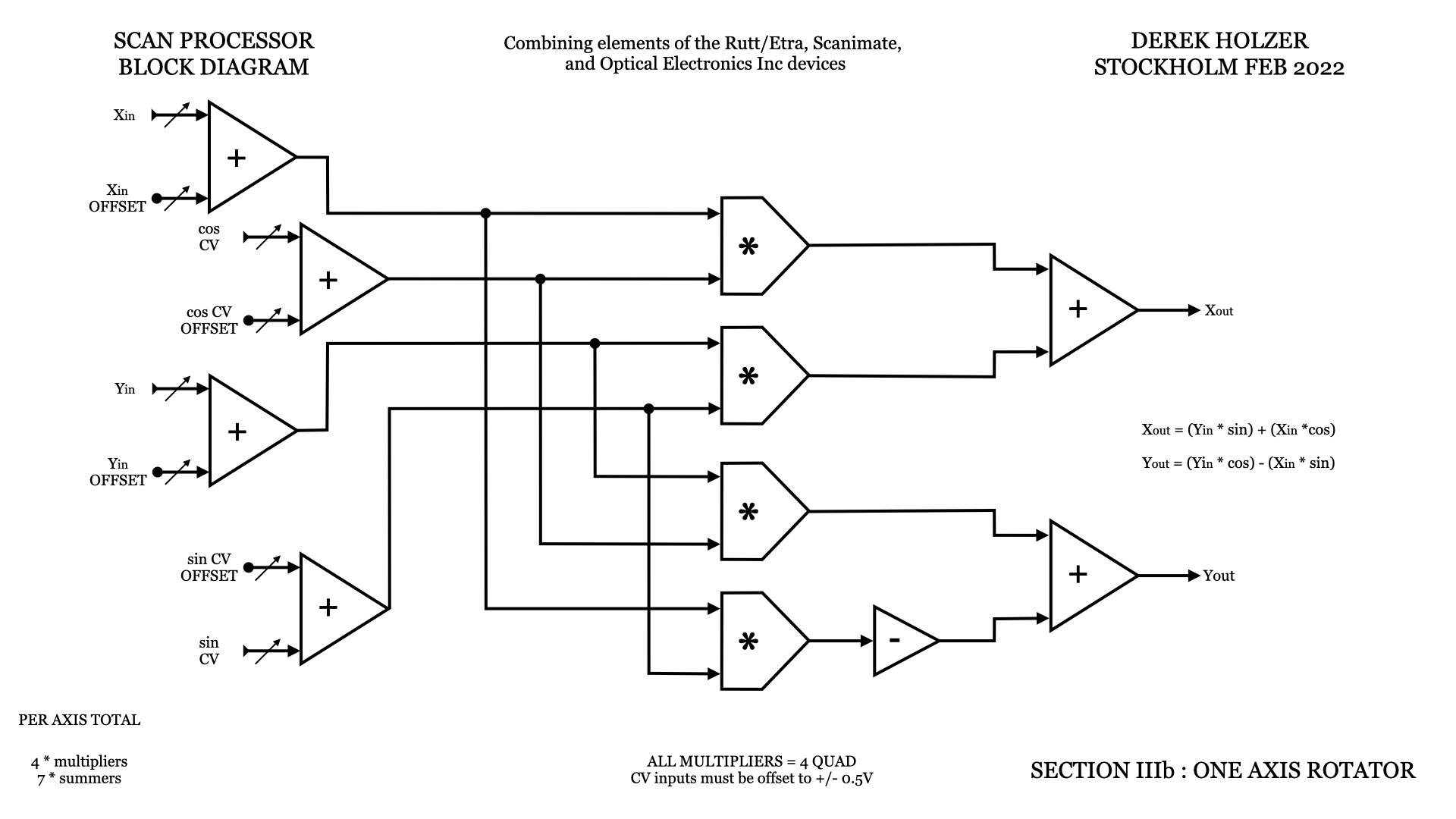
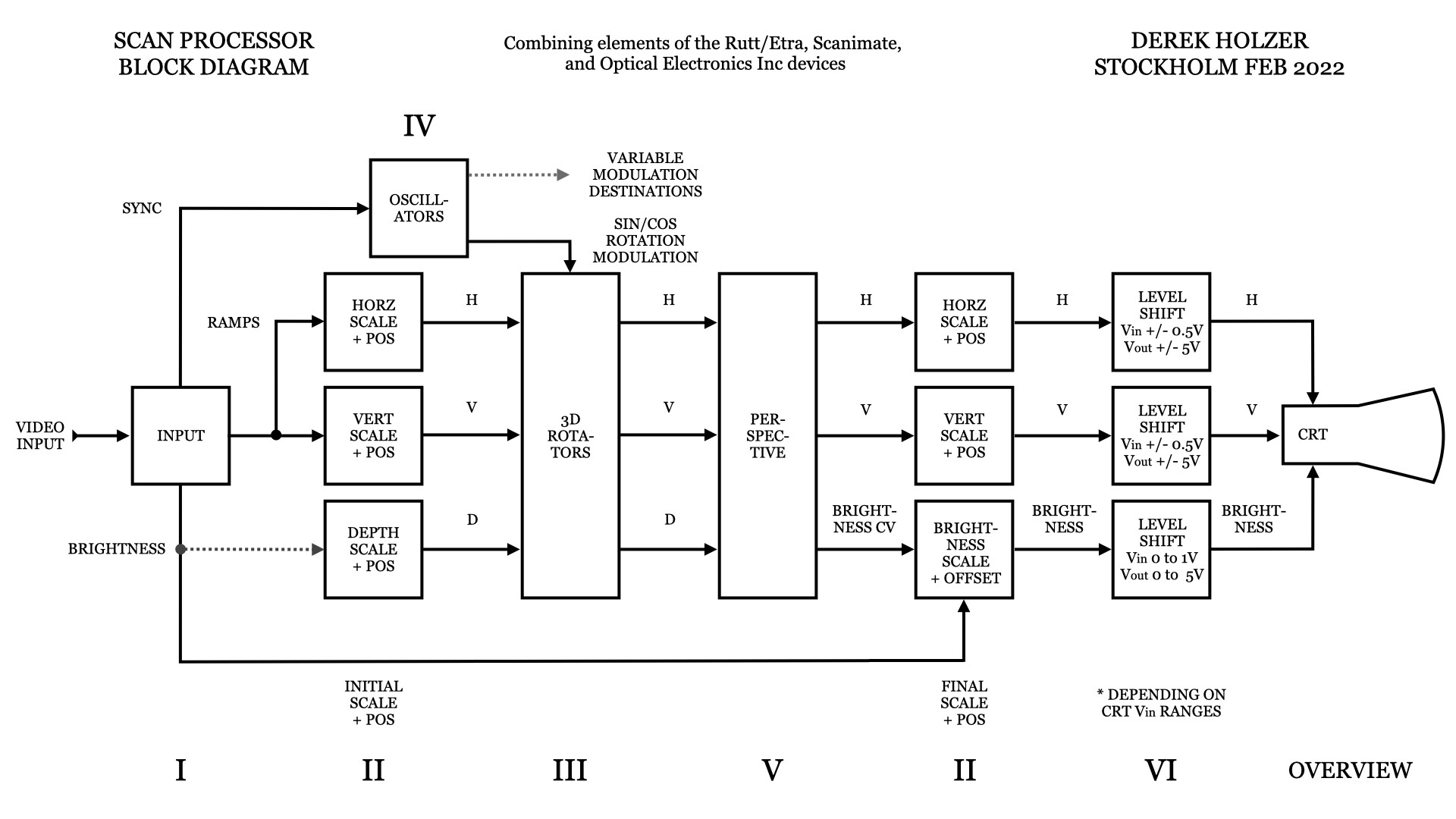
The idea is to be able to manually trim any small voltage offsets introduced by any of the op-amps along the way in each rotator module, since offsets in the signals will shift the center of rotation, and because there will be three rotators in series with any given axis passing through two of them. See block diagram. It seems to me the best way to do this is to make the trimmers bipolar, then we don’t need to fuss with other values in the multiplier.
#4 — transistorcat · 2022-02-24
On second thought, lifting the positive input on U1.2 is probably simpler, but the idea is the same, you don’t need to add a negative reference to shift the offset voltage into a bipolar range.
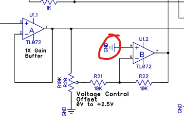
Connecting this node to a resistor divider to 2V5 would shift the offset down. If you want to have a full range of +/-2V5 you’d also have to change R21/R22
#5 — transistorcat · 2022-02-24
Or equivalently just replacing R20,R21;R22 and U1.2 with any attenuverter implementation with a suitable range
#6 — transistorcat · 2022-02-24
Either way, if I’m reading the LT1251 datasheet right, the answer to 1 seems to be yes, and the answer to 2 is that you could get the same result with fewer opamps by doing as suggested above, but i think just inverting the 2V5 for the other end of the offset would also work.
If you do that, you can also swap the inverting buffer for a non-inverting one, since you now have a full range bipolar input to begin with.
#7 — macumbista · 2022-02-24
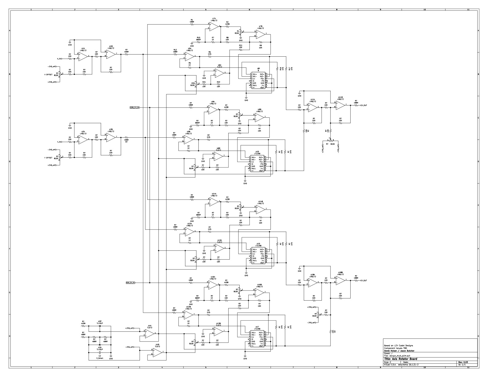
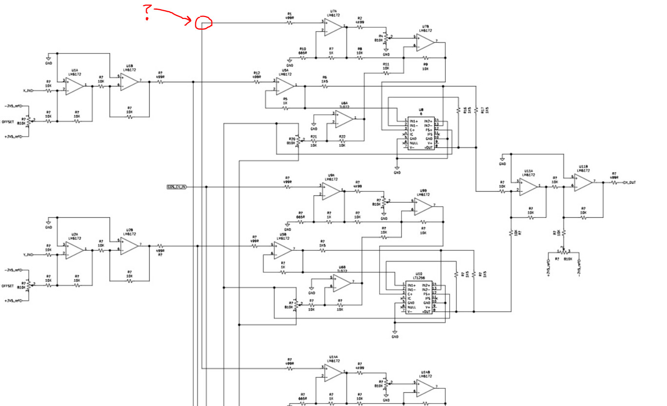
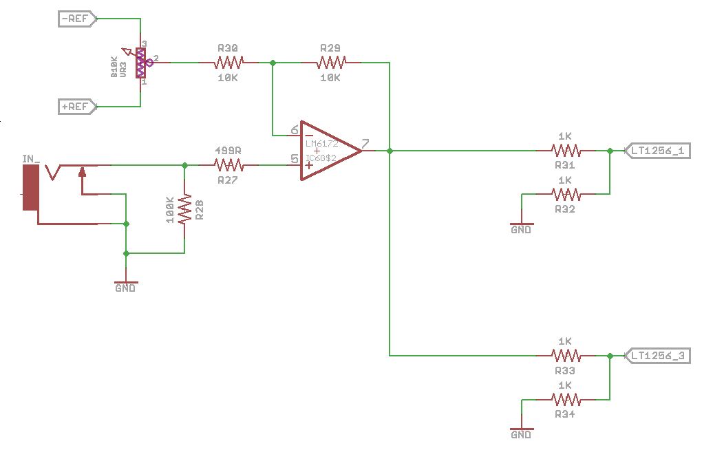
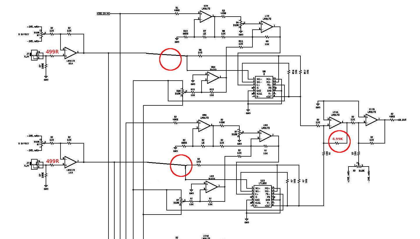
Thx we’ll definitely take those suggestions on board. Here is what we have so far. Warning that this is totally untested yet, just a moshup of two LZX schematics in progress. Comments welcome!
#9 — Fox · 2022-02-24
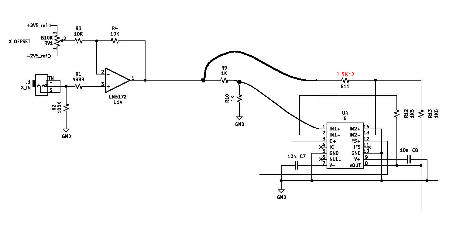
The output pin (pin 7) of your buffer should be the common point from which all subsequent inputs originate. The resistor I placed an X above should be bridged. R12 should remain.
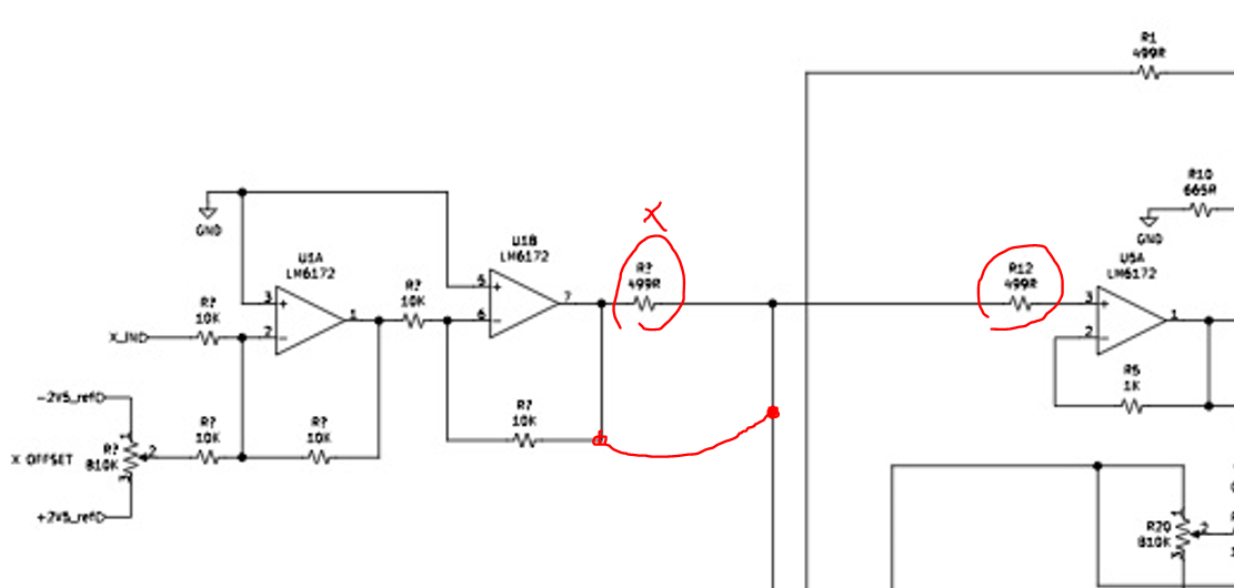
Is “Y_IN” connected directly to a jack? I do not recommend connecting the input jack to the negative input of an op amp. Every video module will have a 470-499 ohm series resistance which will be added to your 10K Series input resistor. The gain will not equal -1 exactly. Use a 100K resistor from your jack to ground and connect it to the positive input of the input buffer.
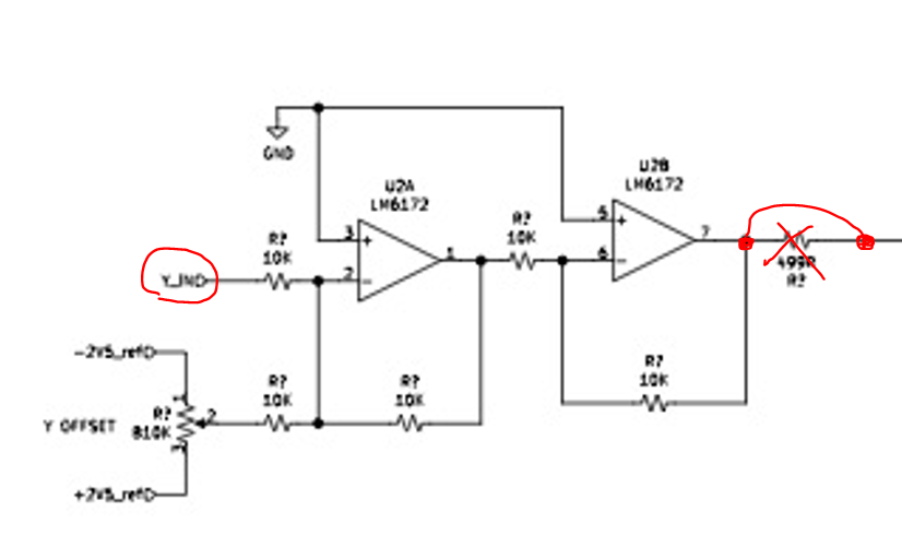
This signal appears to only connect to two op amp inputs:
#10 — Fox · 2022-02-24
macumbista wrote:
If there are four multipliers on each board (plus several op amps), can we buffer a global 2.5V using a single op amp for the entire board?
You may want to, yes. Buffering a single 2.5V reference will grant the benefit of trimming it at one point.
macumbista wrote:
The more complicated question: can we simply op-amp invert the +2.5V from the TL431 to get -2.5V, or should we make a separate TL431 “flipped upside down” to get -2.5V to be buffered by one (or more) op amps?
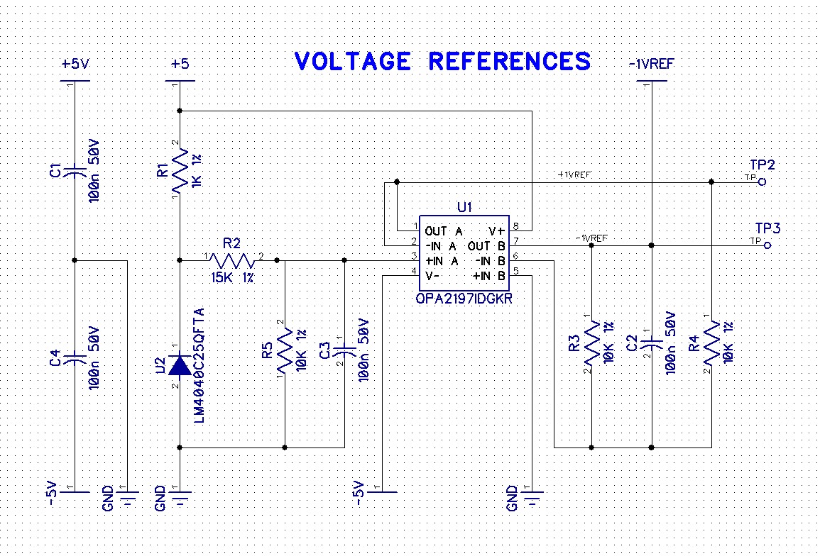
I suggest using one half of a TL072 to buffer the 2.5V signal and the second half to invert it. No need for a second TL431. You may add a trimmer on the feedback pin of the TL431 and another trimmer on the feedback pin of the inverting op amp.
An alternative reference solution was shared by Lars with claims of improved noise.
#11 — Fox · 2022-02-24
Fox wrote:
This signal appears to only connect to two op amp inputs:
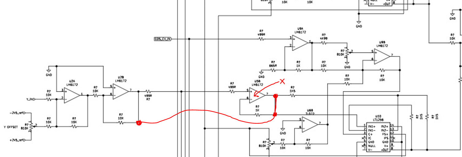
Oh, it looks like the COS_CV_IN and SIN_CV_IN input tags are placed on the same trace.
#12 — JRButcher · 2022-02-24
Thanks - yes, some of those are known issues (opamp in R’s missing, mistakes on input routing) as I was trying to get as much on the page as possible in a short time frame. I do appreciate the tips re: ref voltage and opamp configuration and will post an updated schematic shortly. Thanks again!
#13 — JRButcher · 2022-02-24
Use a 100K resistor from your jack to ground and connect it to the positive input of the input buffer.
If I’m understanding correctly, You’re suggesting an additional non-inverting stage ahead of what is in the drawing (as U1A/U1B) with corresponding resistor omissions - as otherwise including the offset via a non-inv / inv pair would result in an inverted signal on the multiplier input (e.g. U5A)?
#14 — Fox · 2022-02-24
Not an additional stage, no. You may in fact get away with one fewer stages if you add some min/max limiting resistors to the offset pot.
Something like this:
The above will apply a gain of 2x to your input voltage, but this can be brought back down to whatever voltage is necessary at subsequent sections of the circuit.How much offset voltage do you want the pot to make available?
You may also be able to remove this redundant buffer:
(there appears to be one redundant buffer for each LT1256 section)
#15 — Fox · 2022-02-24
Are the X offset and Y offset pots going to be accessible from the front for users or pre-trimmed and not accessible?
#16 — JRButcher · 2022-02-24
Fantastic - I knew I was overlooking something much simpler, and appreciate the suggestion!
I’ll leave it to Derek to chime in re: accessibility of controls, but I believe the plan is to have dual footprints for either pots or internal trimmers.
#17 — macumbista · 2022-02-25
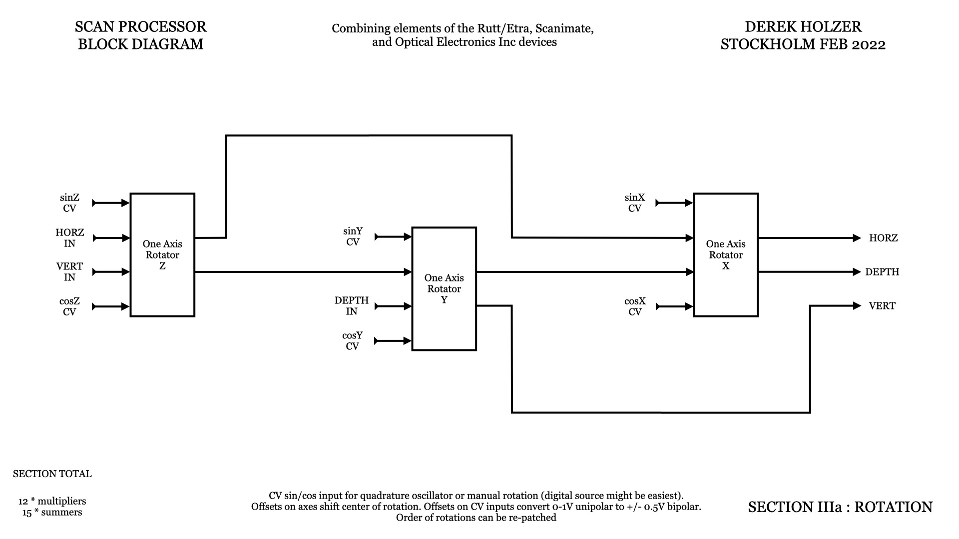
All user accessible scaling and offsetting are done in other parts of the instrument. These rotators should be as simple as possible, trimmed only to get rid of cumulative op amp offsets. See figure.
#20 — JRButcher · 2022-02-25
Feedback appreciated!
#21 — Rik_bS · 2022-02-25
I’d be very interested to see this come to life as a PCB project to build, even if it required custom front panel and wiring.
That said, would also be very grateful if it was taken further

#22 — Fox · 2022-02-26
macumbista wrote:
All user accessible scaling and offsetting are done in other parts of the instrument. These rotators should be as simple as possible, trimmed only to get rid of cumulative op amp offsets. See figure.
I assumed they were supposed to be hand trimmed before use, not as pots. The precision appears to be very important here.
JRButcher wrote:
Feedback appreciated!
I’ll look it over more thoroughly again shortly.
Consider this, if you work with the voltage as +/-1V instead of +/-0.5V, then you can attenuate the signal at the end instead of 4-times before the LT1256’s. Four of the buffers are redundant. Sorry for the bad photoshopping:
EDIT: Can you double check how the 3rd and 4th LT1256 outputs are mixed together.
#23 — macumbista · 2022-02-26
Yes I will open source anything Jason and I come up with, I’m currently discussing a perspective circuit with Dave Sieg as well.
Blockquote>>>> I’d be very interested to see this come to life as a PCB project to build, even if it required custom front panel and wiring
#24 — JRButcher · 2022-02-26
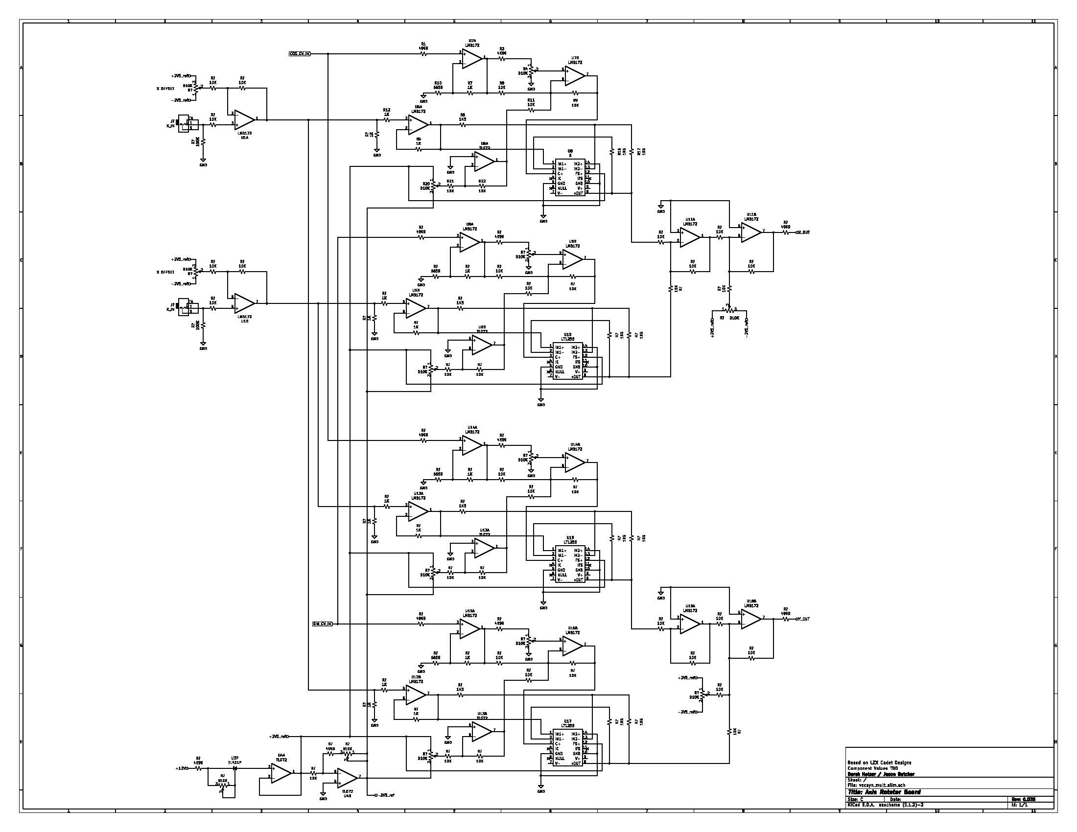
Thanks - very helpful. I was concerned about disturbing the multiplier inputs too much and taking this away from the known quantity that is the Cadet X, but I’ve made the changes you suggested. I did also include the 1K resistor pairs from the input buffer to each multiplier section that you had earlier included.
The output of the 4th multiplier needs to be inverted according to Derek’s diagram, hence the slightly different configuration there in the output section. I did change the resistor values per your suggestion.
I’m in agreement with Derek - happy to make the fruit of the project openly available to anyone that can use it, and very much appreciate the help here in getting this off the ground.
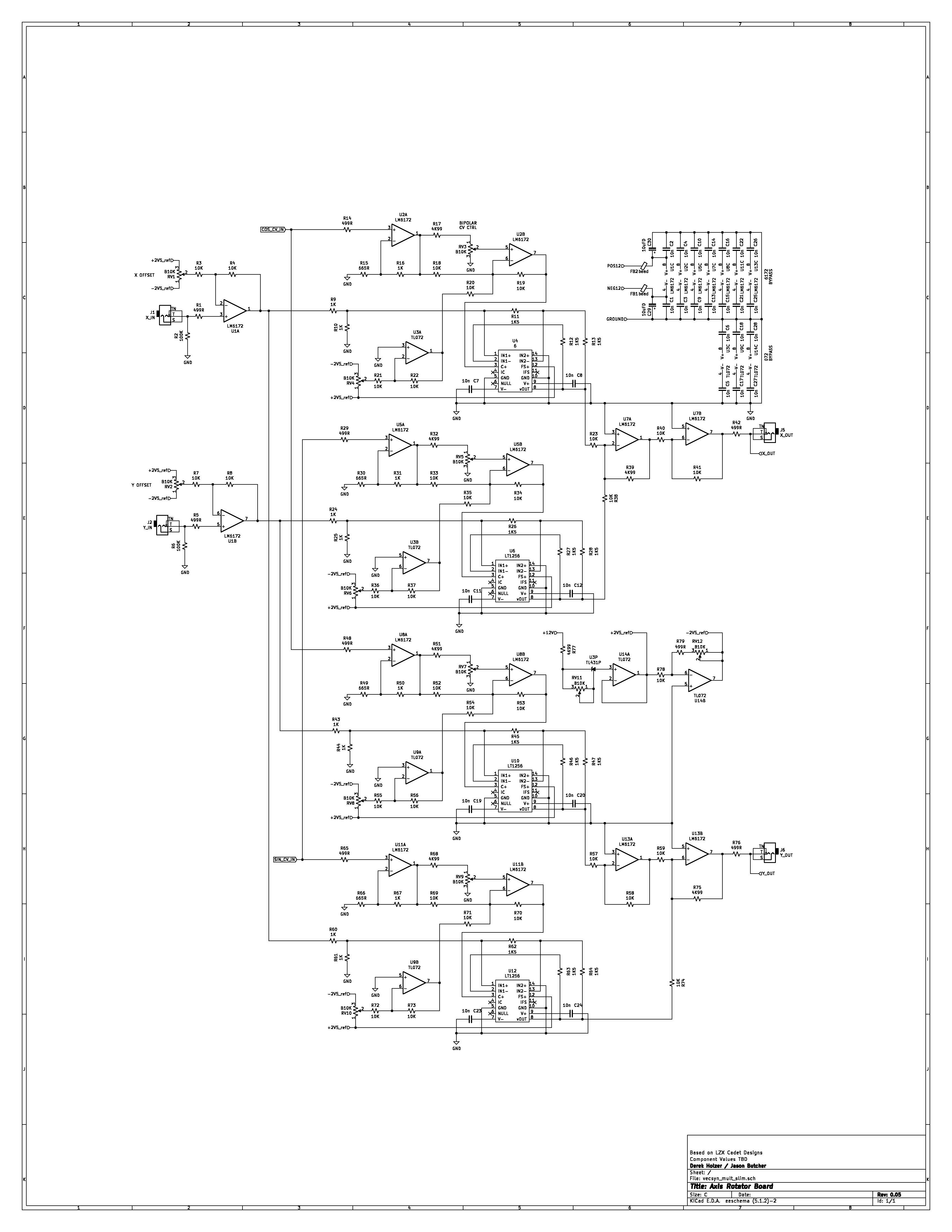
(image edited with updated annotation and then again for bypassing)
#25 — Fox · 2022-02-26
JRButcher wrote:
The output of the 4th multiplier needs to be inverted according to Derek’s diagram, hence the slightly different configuration there in the output section. I did change the resistor values per your suggestion.
Ah-hah, ok.
I noticed a few things that got mixed up with the edits.
Heres how you need to attenuate the signal if you want to do it before the LT1256’s:
I think the TL431 got rotated. The Cathode should connect to the input of the buffer and the Anode should connect to ground.
#26 — meudiademorte · 2022-02-28
Good to hear! Looks very promising