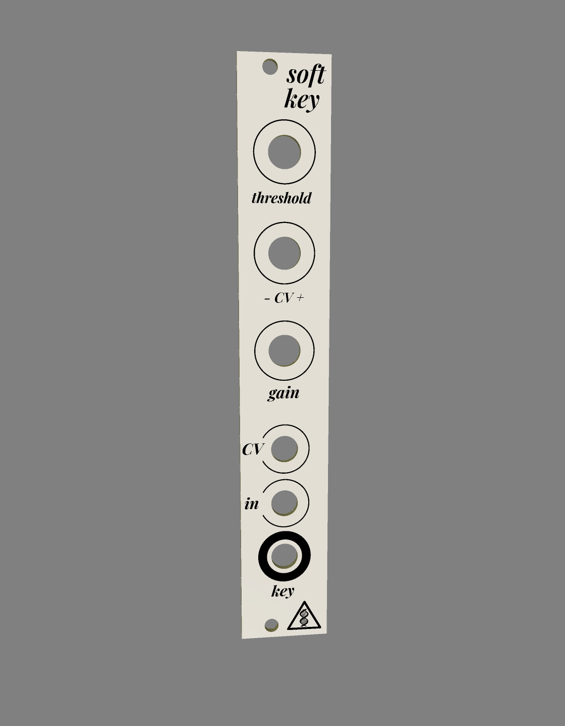
[WIP] DIY Soft Key
Category: Unknown · Tags: — · Posts: 52
#1 — phosphenes · 2022-10-26
Hi All
Since @creatorlars very kindly shared a soft keyer block diagram I’ve been playing about with simulations and started breadboarding a soft key with the goal of putting a DIY module together.
I wanted to see what the community thought about HP size versus functionality. Do I keep it to 4HP and create just a simple soft key module which can then be patched to a VCA fader? Or would you prefer to have an integrated VCA and the relevant controls for a soft keyer in say 6-8HP?
I currently use mostly 4HP DIY video modules and have plenty of spare VCAs in the rack so 4HP makes sense for me but very interested to hear everyone’s thoughts.
#2 — rempesm · 2022-10-26
More HP so you can fit Gain and Threshold pots on it with associated CV input / attenuverters on both controls.
#3 — Rik_bS · 2022-10-26
Integrated IMO, so we’re not needing another VCA
#4 — Analogmonster · 2022-10-28
A 3rd vote for more hp+more features here
#5 — saiteron · 2022-10-30
4th vote for the same

#6 — imageofsin · 2022-11-02
1st vote for 4hp
sorry ya’ll i’m just into modular synths for their… modularity

#7 — Analogmonster · 2022-11-08
I will elaborate a little. I’m not aware of a 2HP VCA, so if you had 4HP soft key without onboard VCA I am going to need another 4HP for an extra VCA to make it work, and we all know the pain of wanting more HP.
6HP is still a compact size, perfect width for a single column of full size alpha pots (I hate the Song Huei 9mm trimmer pots, too much wobble) and 2 columns of jacks. Also 4HP modules next to each other with full sized pots can get in the way of those born with sausage fingers!
I personally never have enough VCAs though
#8 — phosphenes · 2022-11-08
I’ve come from the Cadet / Castle world of 1 function per 4HP, so my initial idea was just a soft key version of the Cadet VIII Hard Key generator but definitely understand the desire to have more functionality in 6HP.
Will hopefully have some time for breadboarding soon, reasonably happy with my circuit sims so far.
#9 — phosphenes · 2022-11-08
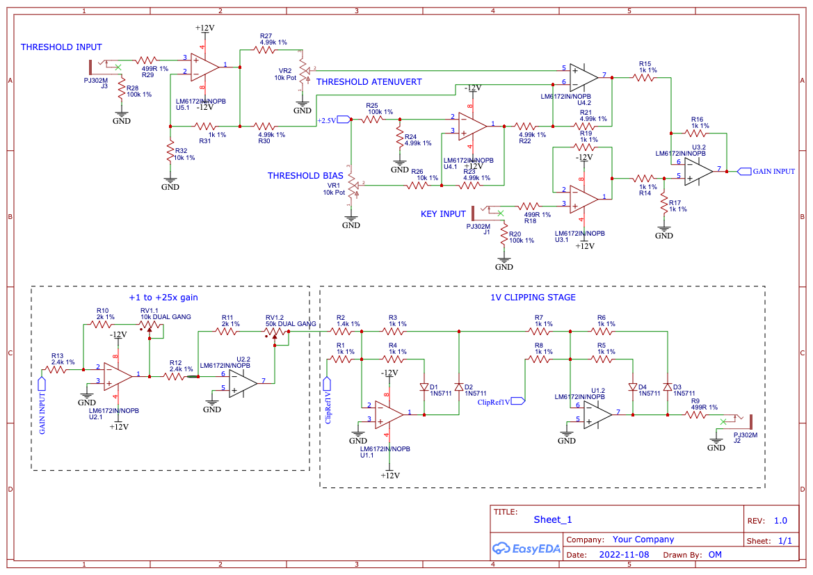
Here’s my current working schematic for the key generator (without any internal VCAs yet). Would really appreciate people digging in and critiquing! I’ve taken the majority of the blocks from different Cadet schematics, the precision clipper from Cadet II, the threshold input and attenuverter from Cadet VIII Hard Key. U3.2 is the differential amplifier for keying the input against a threshold voltage.
Following Lars’ recommendation I’ve implemented the gain control in two stages, from roughly x0.69 to x25.
I’ve not included circuitry for power, 1V and 2.5V reference voltages. U4.1 can be swapped for a non-video op amp, just copy and pasted for ease in this early version.
#10 — Fox · 2022-11-08

I see a few things to note:Your threshold input and key input jacks have the ground pin connected through a 100K resistor instead of the resistor terminating the input signal.
The output jack, J2, should be connected to the other side of the clipping diode.
I also suggest tying your input jack switch pins to ground as the LM6172’s have a nasty input bias when just terminated through 100K.
EDIT: I think your dual gang pot shows two values, 10K and 50K (?)
EDIT2: ooh. Lars must have suggested two gain stages for an non-linear gain curve. Interesting.
#11 — phosphenes · 2022-11-09
Thanks Fox! All great shouts.
creatorlars wrote:
I haven’t published a reference circuit, but a block diagram is fairly straightforward.
Here’s how I do it after trying many ways:
>>>> I tried lots of specialty high gain parts or integrated high gain VCA parts that were expensive and troublesome over the years. What works best in the end is just doing multiple stages after the VCA block, with 4x - 5x per gain stage, and use a separate op amp per stage. Two 5x stages in series it gives you a total gain of 25x, which gets a decently hard edge without going too crazy (this is about where Topogram sits for example.) Cadet II RGB Encoder is a good reference for a precision Black/White clipping circuit.
#12 — syntonie · 2023-01-19
The module concept and schematic looks great!! You may have figured it out already, but you need to make R2 1k instead of 1.4k as it is done in the Cadet RGB encoder circuit, as the 1.4k value is here to reduce the 1V level input to about 700mV, so it is then scaled properly for the AD724, whereas here you’d like to keep your signal 0-1V I suppose.
#13 — phosphenes · 2023-01-19
Thanks Bastien, yes I’ve corrected that now. Thanks for the thread bump, Christmas took over and I completely neglected this project, need to pick this back up again!
#14 — creatorlars · 2023-01-20
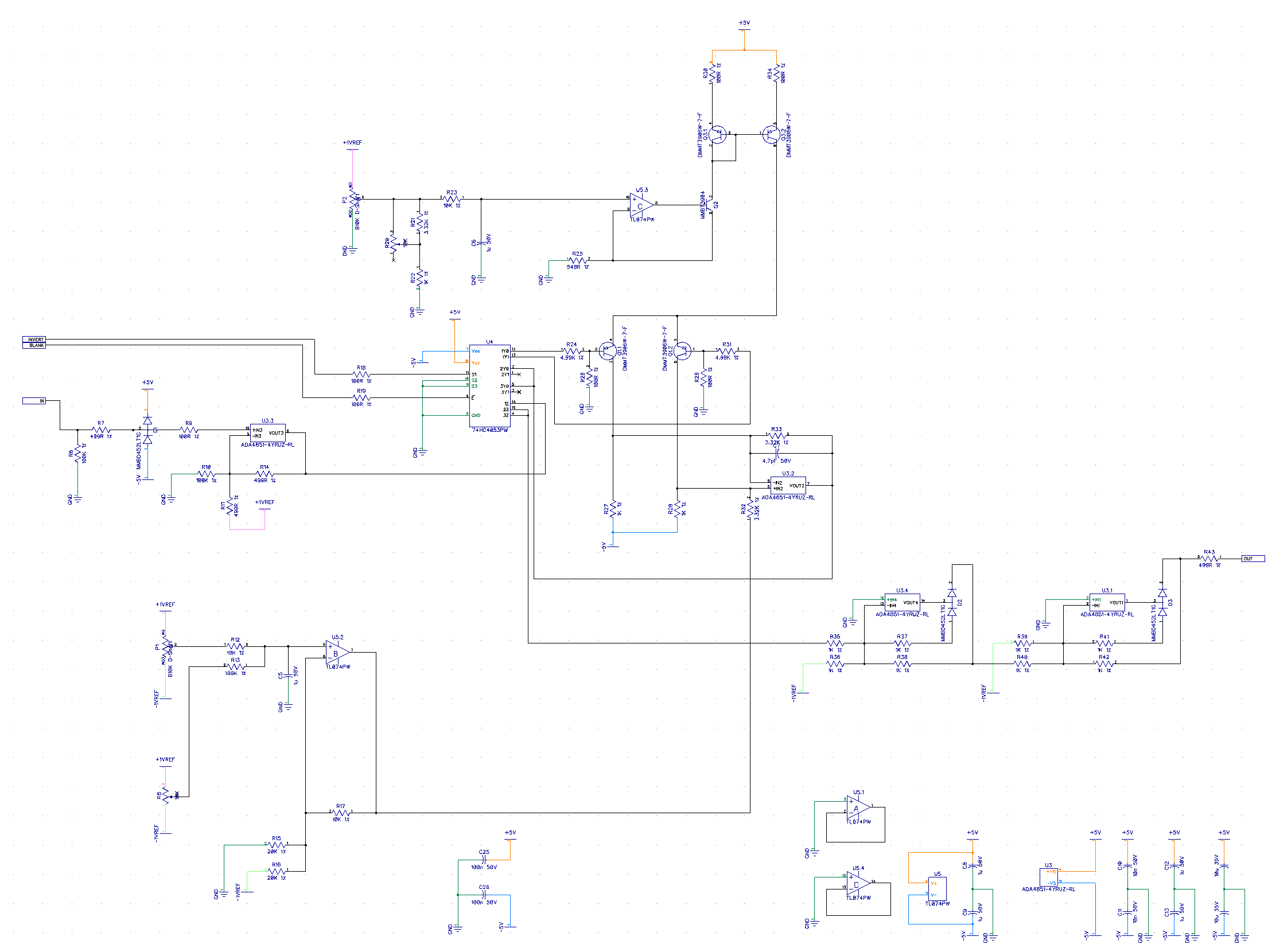
Good work @phosphenes !
The output tap is in the wrong place. Add a unity gain buffer at junction of R6 and D3. Good idea to simulate it with SPICE (at least the bottom half of your design.)
I’m not sure about the dual gang pot in line with the gain setting resistors – maybe put a high value across it (1M) just in case a resistive element in the pot has an issue, it makes sure the circuit will have some known value.
Here is one channel of the ESG3 processor for a reference design, which is effectively a soft key gen with a range of 0-4X.
#15 — Jefro · 2023-01-20
Just to play devil’s advocate, I’d like to see another standalone video VCA. I have the BSO TVVCA, and really wish I had another.
At the same time though, having one integrated would also be nice.
#16 — rempesm · 2023-01-20
You can get the Cadet Multipliers printed right now if you want:

github.comhttps://github.com/lzxindustries/lzxcadet/tree/main/C10main/C10
LZX Cadet Series EuroRack Video Synthesizer DIY Modules
Link: lzxcadet/C10 at main · lzxindustries/lzxcadet
2Q mode on Cadet Multiplier is a standard VCA.
#17 — phosphenes · 2023-01-26
Just thinking about PCB layout, thinking about 4 layer boards to try and help with noise on the high gain settings. How do people feel about the higher cost of a DIY 4 layer PCB?
#18 — Marizu · 2023-01-27
What kind of difference would it make?
I’m assuming there are a few other pricey components on there. Would it make a big percentage difference to the cost of the completed unit?
Would it mean that it could function better in a HD environment? HD Ready

#19 — rempesm · 2023-01-27
It would likely reduce visible noise if all the other layout considerations are made. Soft keyers inherently need to use high gain which will amplify any noise that exists in the circuit pre-gain. Separate power planes can help with this and seems to be one of the several major design changes with Gen3.
Marizu wrote:
Would it mean that it could function better in a HD environment? HD Ready
What would prevent it from working in a HD environment? If it doesn’t have a sync connection, it will pass signals because there’s no timing format issues to consider. I don’t think that the overall bandwidth of the LZX universe has changed with Gen3–virtually the same op amps from Expedition are being used throughout. Every module is arguably HD ready if it its operation isn’t dependent on timing formats, like Memory Palace or Diver, etc.
The question of fidelity of the output it passes is a whole other issue. I don’t think useful metrics have really been defined for the community to weigh in on that objectively yet.
This comment isn’t specific to @phosphenes’ project but is more about all modules in the video universe these days since we have access to multi-format encoders now.
Seeing folks get rid of useful modules in their rig because the maker doesn’t specifically say it’s “HD ready” without any qualification of what that really means has been sad to see.
#20 — Marizu · 2023-01-27
I appreciate that it doesn’t have a sync.
I wondered whether using a four layer board would reduce the noice in a way that would make the design more appealing to people that are working in a HD workflow.
I had, possibly incorrectly, assumed that with a higher definition image, small amounts of noise would be more visibly apparent than in a standard definition image.
#21 — Robbertunist · 2023-01-27
Great to see the regular posts on here @phosphenes

I’d happily pay extra for a 4-later PCB, especially if you prototyped a 2-layer & saw a noticeable difference, even if only a slight one.
I’d suggest using the standard 4 op smt op-amps used in most non-TH (through-hole) designs, I’ve forgotten the name but it’s similar to ADA4851-4. Presoldered would be lovely, & again, I’d pay extra for that.
The LM6172 has become to expensive in my opinion.
#22 — phosphenes · 2023-01-27
I’m definitely intrigued to see the difference between a 2 layer and 4 layer on a DIY build, probably a worthwhile experiment for the DIY community in general. I do wonder if the benefits of the layer stack up would be insignificant compared to the issues introduced by through-hole components etc.
I’m going to stick designing with the LM6172 for the time-being because its what I’m used to but I do take your point, I’d love to be in a position to offer pre-soldered SMD but that feels a bit further down the road for me!
#23 — creatorlars · 2023-01-27
I would definitely go for a 4 layer PCB, whether it’s thru-hole or not. Just design a 2-layer board like you normally would, but make the 2 inner layers 100% coverage ground planes, instead of routing ground as traces. It’s like a big blanket of insurance for cross talk and signal integrity. 4 layer boards are so cheap these days there’s not a good reason to avoid them, in my opinion.
#24 — creatorlars · 2023-01-27
rempesm wrote:
I don’t think that the overall bandwidth of the LZX universe has changed with Gen3–virtually the same op amps from Expedition are being used throughout.
The statement about op amps is correct! Where bandwidth has improved with the Gen3 modules, it’s because of the switch to active attenuverter and switch circuits (the video signal never goes through a passive resistive element like a potentiometer or toggle switch.) So it would be correct to say that the modulation bandwidth (whenever the signal goes thru an attenuverter) has been improved, but the base signal path is almost identical.
Seeing folks get rid of useful modules in their rig because the maker doesn’t specifically say it’s “HD ready” without any qualification of what that really means has been sad to see.
Agreed, this is the exact opposite of what I wanted. I was trying to introduce HD timing options for sync and output – it’s about tempo, not resolution! – and I was trying to do it specifically in a way that existing systems could grow, not be replaced.
#26 — phosphenes · 2023-02-08
Prototype PCBs ordered from JLCPCB tonight! Taking bets on what stupid design mistake I’ve made this time…
#27 — phosphenes · 2023-02-09
So now my 4HP Soft Key prototype is being manufactured I’m turning my thoughts to the design of full Soft Keyer with an integrated VCA and wanted to gather some opinions on functionality.
I’d like to include an internal rectifier circuit to provide an outline function but was wondering about instead just including an ‘effects loop’ style input and output where any function could be patched into the key signal path, any preference?
I’m basing the VCA circuit on the Cadet Fader VI circuitry around the LT1251 (because of its snap to zero functionality), this is a 2Q VCA, I can’t see any benefit to having the option of switching between 4Q but wanted to see if anyone else had any suggestions.
#28 — Fox · 2023-02-09
phosphenes wrote:
I’d like to include an internal rectifier circuit to provide an outline function but was wondering about instead just including an ‘effects loop’ style input and output where any function could be patched into the key signal path, any preference?
The effects loop i/o is a pretty novel idea. My vote is for that.
phosphenes wrote:
I’m basing the VCA circuit on the Cadet Fader VI circuitry around the LT1251 (because of its snap to zero functionality), this is a 2Q VCA, I can’t see any benefit to having the option of switching between 4Q but wanted to see if anyone else had any suggestions.
Were you planning on using the VCA to fade between a “foreground” and “background” image or were you thinking of using it as a fade-to-black multiplier?
I would just recommend 2Q.
#29 — Analogmonster · 2023-02-11
Great idea with the fx loop, best of both worlds - VCA is there but can patch in-between if you want it. BTW JLCPCB do aluminium PCBs now and they are a very good price. I just got back an order for black PCB with white silkscreen, perfect for front panels
#30 — phosphenes · 2023-02-16
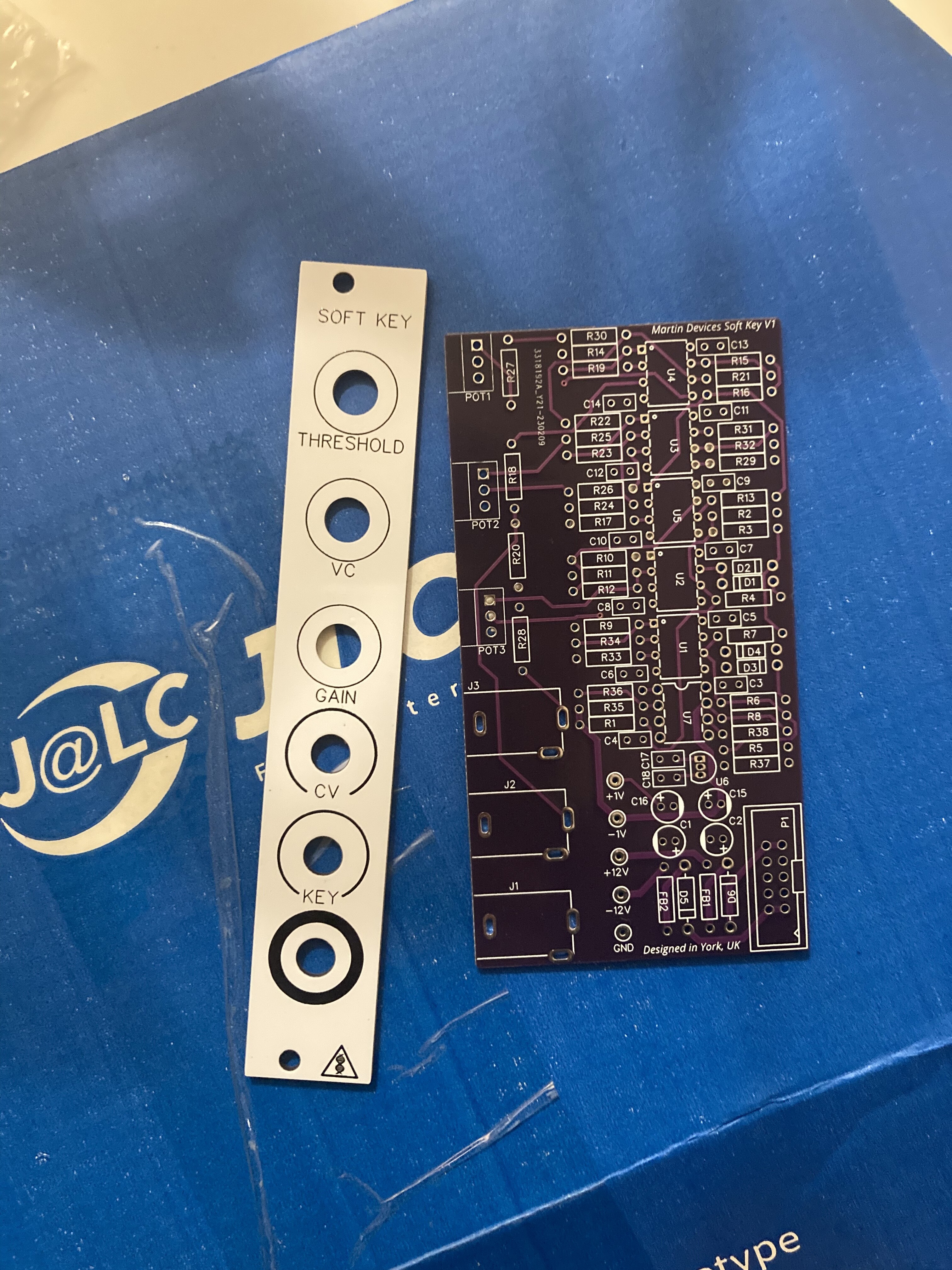
Prototype PCB is here, will build and test this weekend, please keep your collective forum fingers crossed for me!
I’m aware that the front panel is pretty dull and the pots and jacks need better spacing on the next version, I just wanted to keep the main PCB to under 100mm to keep the cost down.
#31 — Fox · 2023-02-16
A tracing job after my own heart! Minimal vias show me that you put in a lot of care.
Did this end up being 4-layers with internal ground planes?
#32 — Fox · 2023-02-16
May I see what your reference(s) buffer looks like in the schematic?
You may not want to populate those electro caps if they’re on the output of the TL072, but I want to have a look at it before making that statement.
#33 — phosphenes · 2023-02-16
Thanks so much, means a lot! Yes 4 layer with internal ground planes.
#34 — phosphenes · 2023-02-16
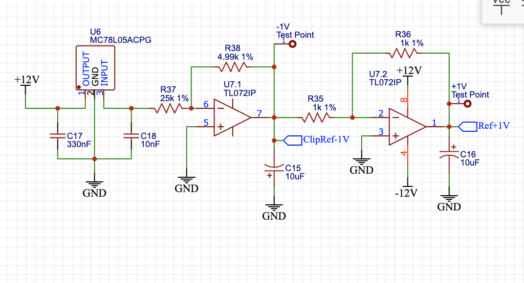
Here’s the reference section, what do you think? I don’t actually use the 1V reference in this circuit, but put it in anyway because I had the spare Op Amp and will use it in the Keyer with integrated VCA.
#35 — Fox · 2023-02-16
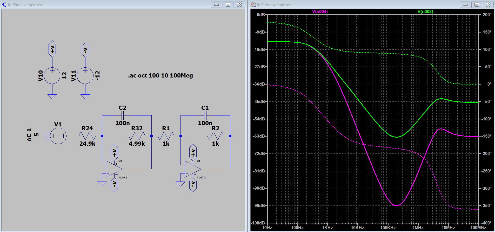
Ah-hah, I see. I suggest that you do not populate C15 and C16 but filtering the reference is important.
10uF may be too high a captivate load for the TL072 to drive. Instead, I would suggest placing small caps in parallel with R38 and R36. The cutoff may be calculated by:
fc = 1/(2piRC)
Where “R” is your feedback resistor. R38 and R36 on your board.
Check out this AC analysis:
And here is an example Lars has shared:
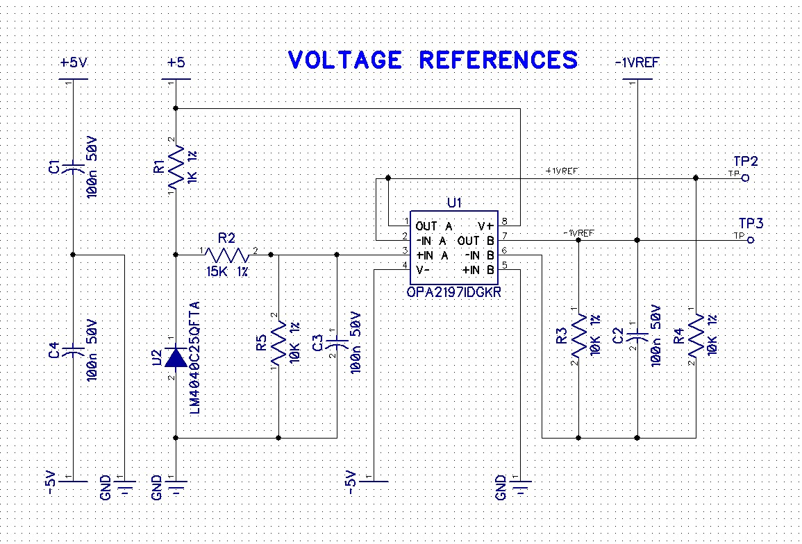
Another observation is the labelling of your 78L05’s pinout. It shows output and input switched, but maybe your silkscreen is correct.
Is the 7805 used for powering any IC’s? If not, a TL431 or LM4040 reference may be better choices. If the 7805 is used for power, then it should be fine.
#36 — phosphenes · 2023-02-16
Thanks Fox these are really helpful observations. You’re right about the regulator being backwards, thankfully should be fine to flip on the board and switch in the next revision.
Hadn’t considered the capacitive load issue, will add your suggestion in the next version. I really appreciate the insight, analogue electronics design can be such a minefield!
#37 — creatorlars · 2023-02-17
I would consider TL431 or LM4040 – if you are using the 7805 maybe a good idea to have a trimmer to set the reference. R35 & R36 I would make 10K resistors. Smaller resistors are fine but it’s more current loading that you need to have in this case. I also like to have a cap in series with feedback resistors (R38 and R36) to slow down any noise coming in.
#38 — creatorlars · 2023-02-17
Just general design notes on using voltage references: On a design like this, it’s not a big deal because the references are only used a couple of places. But in high gain scenarios where the VREF is distributed across multiple circuit blocks, you have to be very careful that you’re not getting any cross talk between the vref and the gain stages. So it can be better to have localized vref buffers. I ran into this problem on early prototypes of Staircase.
#39 — phosphenes · 2023-02-21
Testing this evening, just scoping things out at low frequency with non-video op amps, just incase I let the magic smoke out of any chips, so it’s a 50p mistake not a £7 mistake. Things are looking good at the moment!
#40 — phosphenes · 2023-03-28
Update - can thoroughly confirm version 1 does not work! Can’t yet confirm why it doesn’t work hahaha
Gain sections and clipping seem to be working but I’m getting no output. Frustratingly the way I’ve laid out the op amps is great for the pcb layout but makes isolating sections more difficult.
Next step is to chop the board up in a more aggressive manner to isolate each sub-circuit and hopefully chase down the issue.
#41 — Robbertunist · 2023-03-29
Shame you didn’t nail it first time but I’d bet a “hole-in-one” is a rare occurrence even amongst very skilled designers once a circuit involves a certain amount of op-amps and a variety in pots & jacks.
Hopefully it’s not U6 causing the issue. This kind of narrow footprint caused me an issue with one of the Castle modules, thankfully it came to life after the 4th reflow & clean up.
Thanks for keeping us up to date with your progress @phosphenes &

you’ll figure out the issue quickly 
#42 — phosphenes · 2023-03-29
U6 definitely isn’t the issue which is nice, voltage reference section is working nicely!
#43 — syntonie · 2023-03-29
Robbertunist wrote:
Shame you didn’t nail it first time but I’d bet a “hole-in-one” is a rare occurrence even amongst very skilled designers once a circuit involves a certain amount of op-amps and a variety in pots & jacks.
Can’t agree more!
phosphenes wrote:
Gain sections and clipping seem to be working but I’m getting no output.
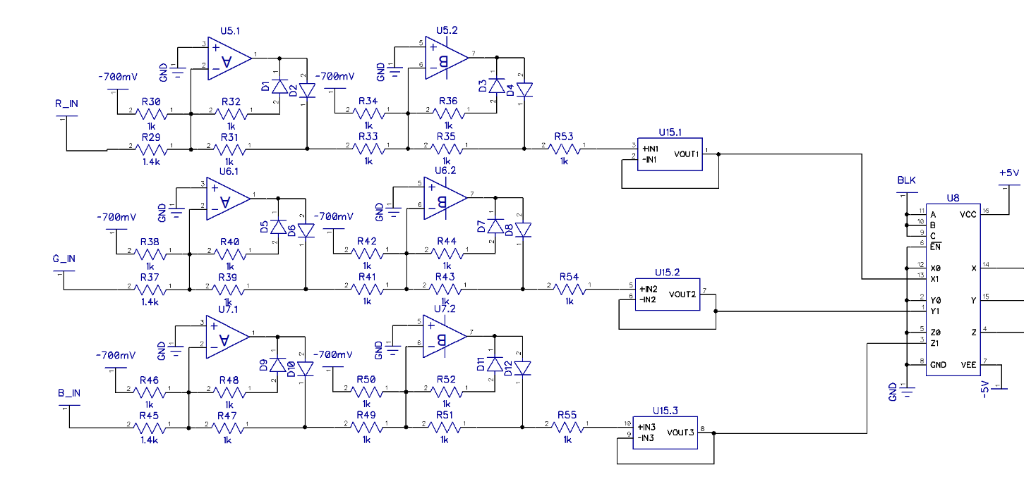
I haven’t paid attention when I first looked at your schematic, but I’m not sure if you can drive the next module input directly at the output of the clipping stage. I had issues with VU007/VU007B taking the output of the RGB clipping section directly to the input of the CD4053 used for blanking as it is done in Cadet II: with hard edged signals and/or signals exceeding 0-1V, it would cause some voltage spike under 0V and above 700mV, which wasn’t an issue at the Composite/S-Video output, cause I guess the AD724 could tolerate some negative/positive excursion. However it caused sync issues on the Component output where the blanked RGB signals are summed together directly using op-amps, as the negative voltage spike present in Y was interpreted as sync by the receiving device, making it glitch. The solution was to use an additional buffer between the clipping section and the blanking section (U15.1/2/3)
When you say “Gain sections and clipping seem to be working but I’m getting no output” do you mean you’re able to see those sections working correctly with a scope, but not when you connect the output to the input of another module? It may sounds like the second clipping stage cannot drive the load, though I haven’t tried driving an output at the output of the clipping stage so I could be wrong.
#44 — phosphenes · 2023-03-29
Hi Bastien, sorry I realise I’ve not uploaded the most up to date schematic, I’ve since added an output buffer from the clipping section. I’ll upload the updated schematic when I get in this evening.
In terms of no output I’m just getting 0V on the output of the buffer.
#45 — syntonie · 2023-03-29
No worries, I had missed Lars comment about adding a buffer at the output at R3/D6 junction, at least you’re sure that it is not what’s causing the issue.
#46 — phosphenes · 2023-03-30
So this is my current clipping and output section. I’ve disconnected R2 from the previous section and connected a signal generator producing a 0-1V sine wave. My test probes are set to 1x. When probing the output I just get +1V DC output. Can anyone see any issue with this section that I’ve missed? Or is it an issue with how I’m testing it? Am I buffering the output incorrectly? Should I be buffering the signal generator before it hits R2?
I’ve isolated the output buffer and it worked fine so can hopefully rule that out?
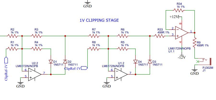
#47 — Fox · 2023-03-30
Looks good to me, simulates correctly too.
#48 — reverselandfill · 2023-03-30
tips:
check your pcb layout file for errors (if you haven’t done so already)
replace IC’s , maybe you got a dud
look where the signal is present and where is is lost. It is possible that there is a solder issue somewhere
#49 — phosphenes · 2023-03-31
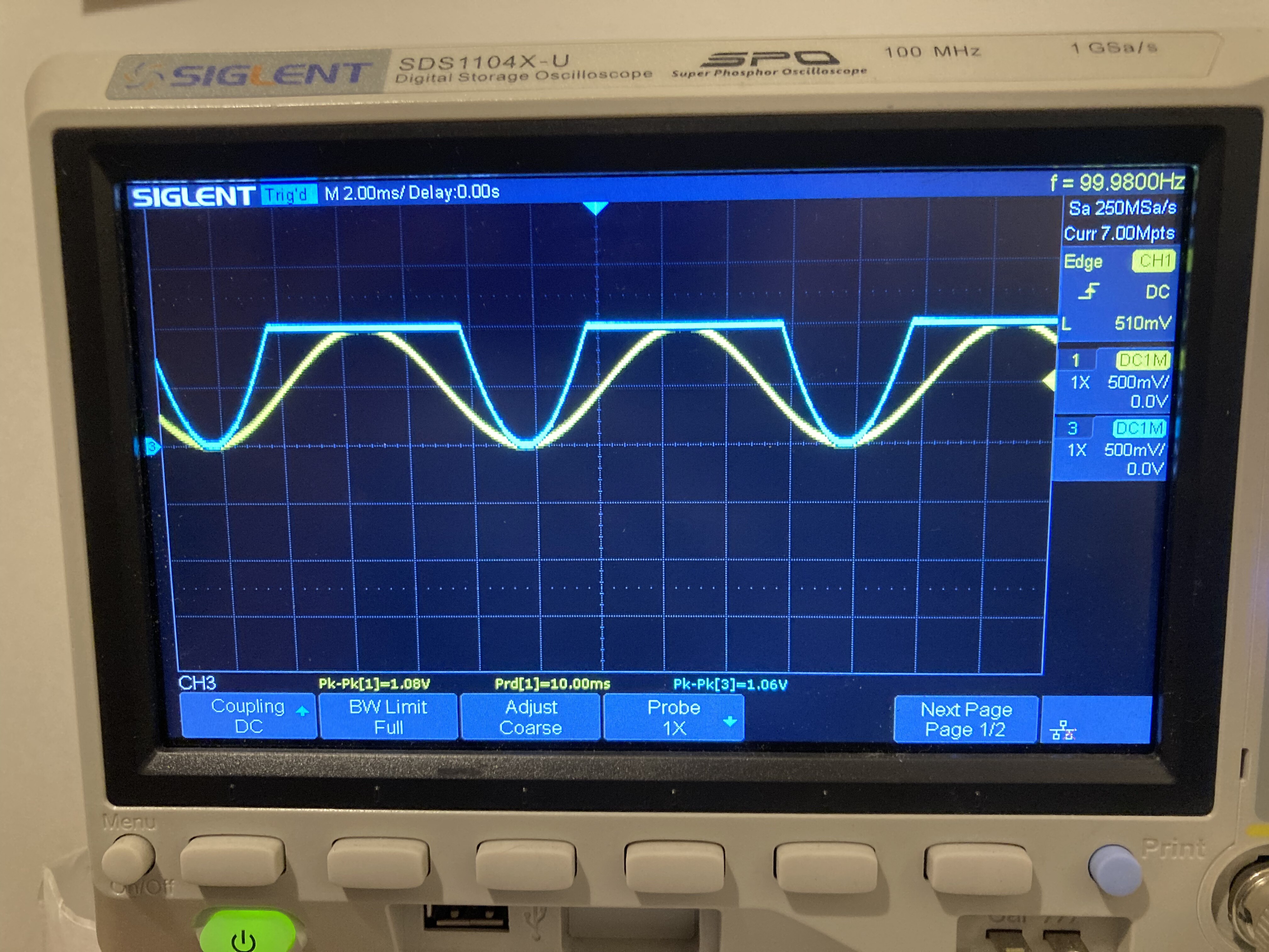
Great advice. Went through every connection to check the PCB, checked the chips then finally discovered R1 was 100R rather than 1k! Swapped out and things are working on the clipping and output sections.
Pictured is some nice asymmetrical clipping!
In my tests I also found I’d got the inputs on one of the op amps the wrong way round in the attenuverter section so next step is to see if I can do a board mod! We’re getting there, albeit slowly

#50 — Jesse · 2023-04-01
creatorlars wrote:
I would definitely go for a 4 layer PCB, whether it’s thru-hole or not. Just design a 2-layer board like you normally would, but make the 2 inner layers 100% coverage ground planes, instead of routing ground as traces. It’s like a big blanket of insurance for cross talk and signal integrity. 4 layer boards are so cheap these days there’s not a good reason to avoid them, in my opinion.
+1
Best practice is a continuous ground plane layer adjacent every signal layer if you have any say in it. The signal doesn’t flow on the traces, it’s a field - and how obnoxious it is depends on your layout. If there’s a ground plane directly below or above your signal trace the field stays tight right under your trace, the return path is in the most efficient route possible. If you don’t leave that gnd space available the field blooms & causes EMI, crosstalk all that nonsense as the return makes a wider loop & rams into everything trying to make it’s way back home.
It’s pretty cool, our universe has autorouting on for return paths by default - just pour a plane & it’ll sort itself out in the most efficient route possible!
I just noticed that if you can swing it you might try to keep it at or under 100mm tall, seems like you can duck the $35 “Engineering Fee” on JLCPCB that way. Think the cutoff is like 102mm or something. Paying that fee isn’t so bad if you’re doing a run but for prototyping OOF!
Awesome work, fun following along

#51 — phosphenes · 2023-04-06
Soft Key Version 2 coming very soon! Will do a final check of everything and then get things ordered this weekend. Once the second version is tested and hopefully working I’ll be ready to do a batch of orders if people are interested.
#52 — phosphenes · 2023-04-27
phosphenes wrote:
this weekend
Three weeks later, just ordered the V2 boards!
#53 — phosphenes · 2023-06-07
Another update, managed to put the wrong gerbers in when I ordered v2, so ended up with another batch of v1… either way I’ve reordered v2 boards today so fingers crossed I should be in a position to offer boards for sale in a month or so!
I’ve been playing about with values on the V1, I’ve swapped out the linear 10k pot on the gain control for a logarithmic 10k and much prefer the level of control it gives over shape.